1. Introduction
_The Serial Peripheral Interface (SPI) is a synchronous serial communication interface specification used for short-distance communication, primarily in embedded systems. The interface was developed by Motorola in the mid-1980s and has become a de facto standard. Typical applications include Secure Digital cards and liquid crystal displays. SPI devices communicate in full duplex mode using a master-slave architecture with a single master. The master device originates the frame for reading and writing. Multiple slave-devices are supported through selection with individual slave select (SS) (sometimes called chip select (CS)) lines. (https://en.wikipedia.org/wiki/Serial_Peripheral_Interface)_
The screenshot below represents the reading of a 16-bit data from the LPS25H pressure and temperature sensor. As you can see, the transaction is performed with only 3 bytes being involved, corresponding to 24 clock cycles (2 times less than with I2C for the same transaction). The price to pay is that SPI requires more wires between master and slave :
- SCK : the bit clock
- MOSI : Master Out / Slave In, used by the master to send data to the slave
- MISO : Master In / Slave Out, used by the master to receive data from the slave
- CS : Chip Select, driven by the master to select a slave among other sharing the same SCK, MOSI, MISO lines
Compare to I2C, SPI protocol is simpler, and faster. It only requires more I/O on the MCU wside.
2. SPI Peripheral Initialisation
The code below is an example of SPI1 peripheral configuration for a master, 8-bit, SPI controller role.
Main concerns when initialising SPI peripherals are:
- Configure pins associated with bus lines (SCK, MISO, MOSI) with correct alternate function
- Make sure SPI mode complies with slave datasheet regarding the sampling clock edge. This is done by tuning CPOL and CPHA configuration bits
- Set the bus speed using the clock prescaler
- For the master mode, disable any hardware management of the NSS (internal CS function)
Add this function to your bsp.rs:
/*
 * bsp_spi1_init()
 * Initialize SPI1 peripheral @375kHz
 */
pub fn bsp_spi1_init(peripherals: &Peripherals) {
    let (gpiob, gpioc, rcc, spi1) = (
        &peripherals.GPIOB,
        &peripherals.GPIOC,
        &peripherals.RCC,
        &peripherals.SPI1,
    );
    // SPI_SCK  -> PB3 (AF0)
    // SPI_MISO -> PB4 (AF0)
    // SPI_MOSI -> PB5 (AF0)
    // CS pin -> PC7 (GPIO)

    // Configure PC7 as CS pin

    // Enable GPIOC clock
    rcc.ahbenr.modify(|_, w| w.iopcen().enabled());

    // Configure PC7 as output
    gpioc.moder.modify(|_, w| w.moder7().output());

    // Configure PC7 as Push-Pull output
    gpioc.otyper.modify(|_, w| w.ot7().push_pull());

    // Configure PC7 as High-Speed Output
    gpioc.ospeedr.modify(|_, w| w.ospeedr7().high_speed());

    // Disable PC7 Pull-up/Pull-down
    gpioc.pupdr.modify(|_, w| w.pupdr7().floating());

    // Idle state is high
    gpioc.bsrr.write(|w| w.bs7().set());

    // Configure PB3, PB4, PB5 as SPI1 pins (AF0)

    // Enable GPIOB clock
    rcc.ahbenr.modify(|_, w| w.iopben().enabled());

    // Configure PB3, PB4, PB5 as AF mode
    gpiob.moder.modify(|_, w| {
        w.moder3()
            .alternate()
            .moder4()
            .alternate()
            .moder5()
            .alternate()
    });

    // Connect to SPI1 (AF0)
    gpiob
        .afrl
        .modify(|_, w| w.afrl3().af0().afrl4().af0().afrl5().af0());

    // Enable SPI1 Clock
    rcc.apb2enr.modify(|_, w| w.spi1en().enabled());

    // Configure SPI with default config
    // 4-wire = full-duplex (MISO/MOSI on separated lines)
    // 8-bit, no CRC, MSB first
    // CPHA = 0, CPOL = 0 -> SPI mode 0 (first clock rising edge)
    spi1.cr1.reset();
    spi1.cr2.reset();

    // Set the baudrate to 48MHz /128 = 375kHz (slow, but easy to debug)
    spi1.cr1.modify(|_, w| w.br().div128());

    // Set data size to 8-bit
    spi1.cr2.modify(|_, w| w.ds().eight_bit());

    // Set as master (SSI must be high), with software managed NSS
    spi1.cr1
        .modify(|_, w| w.mstr().master().ssi().slave_not_selected().ssm().enabled());

    // Enable SPI1
    spi1.cr1.modify(|_, w| w.spe().enabled());
}
Now try this in the main function and capture the SPI transaction using 4 oscilloscope channels wired to SCK, MOSI, MISO and CS:
#[entry]
fn main() -> ! {
// Get peripherals
let peripherals = Peripherals::take().unwrap();
let spi1 = &peripherals.SPI1;
// Configure System Clock
let _fclk = system_clock_config(&peripherals).unwrap();
// Initialize LED pin and USER Button
bsp::bsp_led_init(&peripherals);
bsp::bsp_pb_init(&peripherals);
// Initialize Debug Console
let mut console = bsp::bsp_console_init(&peripherals);
print!(console, "\r\nConsole Ready!\r\n");
print!(console, "SYSCLK = {}Hz\r\n", _fclk);
// Initialize I2C1 peripherals
bsp::bsp_spi1_init(&peripherals);
// Try and send something
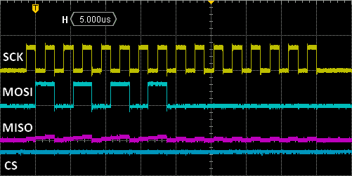
spi1.dr.write(|w| w.dr().bits(0x55));
// Main loop
loop {}
}
If everything goes well, you'll get this:
The above snapshot confirms:
- that we've suceeded in configuring GPIO alternate functions to work with SPI1
- that writing to the SPI_DR register fires the SPI transaction up
- that clock frequency is as expected (375kHz)
- that the 0x55 byte is well transmitted on MOSI. Note that 0x55 correspond to the 01010101 binary sequence, which is convenient for debug
- that nothing was transmitted by any slave (MISO stays low)
That's a good start. Yet, although we did configure SPI peripheral to work with 8-bit data, one can see that actually 16 clock cycles have been generated after the loading of the SPI_DR register. Why is that?
The reason is stated in page 758 of the reference manual: _When the data frame size fits into one byte (less than or equal to 8 bits), data packing is used automatically when any read or write 16-bit access is performed on the SPIx_DR register. The double data frame pattern is handled in parallel in this case. At first, the SPI operates using the pattern stored in the LSB of the accessed word, then with the other half stored in the MSB._
In order to avoid the so-called data packing, one should make sure that only 8-bit access is used when writing to the SPI_DR register. And to do this, we need to go unsafe...
You can try this:
unsafe { core::ptr::write_volatile(spi1.dr.as_ptr() as *mut u8, 0x55) }
And you'll get what you want, i.e. a single byte transfer:
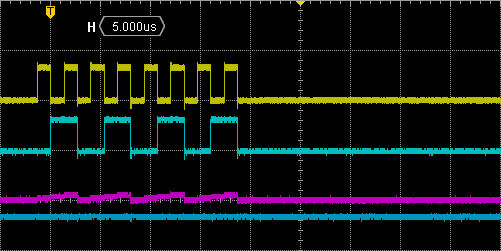
If you're curious about the effect of that specific register casting, you'll need to dig into the assembly code. You'll discover that the writing into SPI_DR is done using the SRTB opcode (forcing byte operation), instead of STR opcode in case of regular writing.
Generated assembly code for classic write:
ldr     r0, .LCPI3_0
movs    r1, #85
str     r1, [r0]
Generated assembly code for unsafe single byte write:
ldr     r0, .LCPI3_0
movs    r1, #85
strb    r1, [r0]
3. Read Transaction
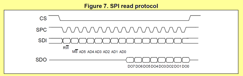
SPI, in full-duplex mode, performs writings (on MOSI) and readings (on MISO) simultaneously every clock edge. Obviously, you first need to tell the slave what operation you want to perform. This is done with the first byte transfer that generally contains fields such as :
- a slave register address (7-bit or less), right aligned
- the nature READ/WRITE of the operation (bit7)
- optional bits depending on slave-specific protocol
Looking at LPS25H datasheet, we can see that:
- register addresses are 6-bit (0-5)
- bit 6 is a MULTIPLE/SINGLE switch indicating whether you want to read/write one or several consecutive registers
- bit 7 is the READ/WRITE switch
Before going any further, again, you'll need to know a little about SPI peripheral flags used to control transactions.
SPI peripheral features 2 FIFO buffers, one for TX, one for RX. These FIFO are 4 bytes deep. Access to the SPI_DR register, actually adds or removes data into/from these FIFOs. The process is transparent, but you need to understand how it works in order to make correct use of status flags. In particular, let us focus on TXE and RXNE flags.
The figure below is a simplified illustration of the SPI behavior. Writing into SPI_DR register puts data to be sent into the TX_FIFO. If it is available (i.e. not currently transmitting), the data is transferred right away into the MOSI shift register, freeing quite instantaneously the TX_FIFO. If the shift register is busy, the data is held into the TX_FIFO (consider this as a waiting queue of data to be sent). If more data are written into SPI_DR, successive TX_FIFO slots are used, up to 4. The TXE (TX Empty) flag signals whether you can add data to the FIFO, or not. It is set when the TX_FIFO is empty, and drops when TX_FIFO reaches half-full (i.e. 2 bytes in the waiting list).
The same thing happens on the receiver side. When a byte is received on the MISO line, it is first put into the RX_FIFO waiting list. You can poll the RXNE (RX Not Empty) flag to know if there is something to gather in the RX_FIFO. Reading the SPI_DR register removes the oldest data from the RX_FIFO waiting list. You can program the RX_FIFO threshold so that RXNE is raised when RX_FIFO contains 1 (FRXTH=1) or 2 (FRXTH=0) bytes.
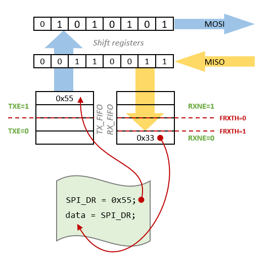
The easy way to handle SPI transactions, when throughput is not an issue, is to do the following for each single byte to be transferred (to/from) the slave :
- Make sure TXE is set
- Write data to be sent into the SPI_DR register. That will start an 8 clock cycles transaction on both MOSI and MISO
- Wait for RXNE to be set. This will occur after the 8th clock cycle
- Read received data from SPI_DR register
Doing so, you're not taking any benefit from the dual FIFO architecture, but it works. Note that RX FIFO threshold MUST be set to 1-byte, so that RXNE flag is raised as soon as one byte arrives in the RX_FIFO.
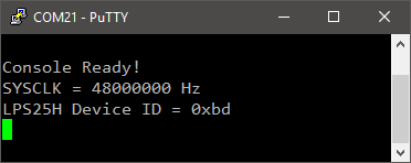
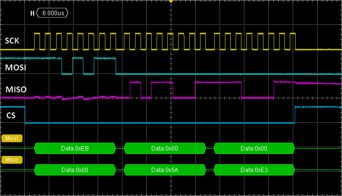
Let us try this approach to read the WHO_AM_I register (address 0x0F) of the LPS25H. The answer should be 0xBD (10111101) according to the device datasheet:
![]()
First, add this function into your bsp.rs library. This function just executes the above 4-step sequence. It takes the byte to be sent on MOSI as argument, and returns the byte received on MISO:
pub fn bsp_spi_send_receive(tx_byte: u8, peripherals: &Peripherals) -> u8 {
    let spi1 = &peripherals.SPI1;
    let rx_byte;

    // Make sure TXE is set before sending data
    while spi1.sr.read().txe().is_not_empty() {}

    // Send tx_byte
    unsafe { core::ptr::write_volatile(spi1.dr.as_ptr() as *mut u8, 0x55) }

    // Wait until incoming data has arrived
    while spi1.sr.read().rxne().is_empty() {}

    // Read data
    rx_byte = spi1.dr.read().dr().bits() as u8;

    return rx_byte;
}
And then, add the code below to the main function. Note that the transaction must be surrounded by software management of the CS pin.
#[entry]
fn main() -> ! {
    // Variables
    let lps25h_id: u8;

    // Get peripherals
    let peripherals = Peripherals::take().unwrap();
    let (gpioc, spi1) = (&peripherals.GPIOC, &peripherals.SPI1);

    // Configure System Clock
    let _fclk = system_clock_config(&peripherals).unwrap();

    // Initialize LED pin and USER Button
    bsp::bsp_led_init(&peripherals);
    bsp::bsp_pb_init(&peripherals);

    // Initialize Debug Console
    let mut console = bsp::bsp_console_init(&peripherals);
    print!(console, "\r\nConsole Ready!\r\n");
    print!(console, "SYSCLK = {}Hz\r\n", _fclk);

    // Initialize I2C1 peripherals
    bsp::bsp_spi1_init(&peripherals);

    // Set FIFO threshold to 1-byte
    spi1.cr2.modify(|_, w| w.frxth().quarter());

    // Select slave (CS -> low)
    gpioc.bsrr.write(|w| w.br7().reset());

    // Send WHO_AM_I register address with READ bit
    bsp::bsp_spi_send_receive(0x0F | 0x80, &peripherals);

    // Send whatever to generate 8 clock cycles and get the response from slave
    lps25h_id = bsp::bsp_spi_send_receive(0x00, &peripherals);

    // Release slave (CS -> High)
    gpioc.bsrr.write(|w| w.bs7().set());

    print!(console, "LPS25H Device ID = {:#04x}\r\n", lps25h_id);

    // Main loop
    loop {}
}
Now you can observe the whole reading transaction:
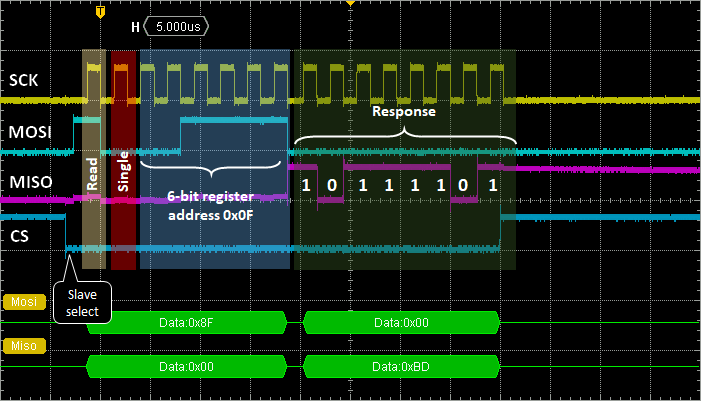
And the corresponding terminal output: