
1. Introduction
Clock settings are of primary importance when you start a new microcontroller project. The way you configure the clocking scheme has direct impact on peripheral programing, application performance and power consumption. This tutorial details the default configuration and provides a function to setup clock for maximum performance and stability. You absolutely need to understand and master the concepts introduced here.
2. STM32 Clock architecture
Open your blink project and edit the main.rs file. Add the following function at the end of the main.rs file:
fn system_core_clock_update(peripherals: &Peripherals) -> u32 {
    static HSE_VALUE: u32 = 8000000;
    static HSI_VALUE: u32 = 8000000;
    static HSI48_VALUE: u32 = 48000000;

    static AHBPRESC_TABLE: [u8; 16] = [0, 0, 0, 0, 0, 0, 0, 0, 1, 2, 3, 4, 6, 7, 8, 9];

    let rcc = &peripherals.RCC;
    let mut system_core_clock: u32;
    let (mut pllmull, pllsource, predivfactor);

    let sws = rcc.cfgr.read().sws();

    if sws.is_hsi() {
        system_core_clock = HSI_VALUE;
    } else if sws.is_hse() {
        system_core_clock = HSE_VALUE;
    } else if sws.is_pll() {
        pllmull = rcc.cfgr.read().pllmul().bits() as u32;
        pllsource = rcc.cfgr.read().pllsrc();
        pllmull = pllmull + 2; // No need to >> 18 because we isolate pllmull value
        predivfactor = rcc.cfgr2.read().prediv().bits() as u32 + 1;

        if pllsource.is_hse_div_prediv() {
            /* HSE used as PLL clock source : SystemCoreClock = HSE/PREDIV * PLLMUL */
            system_core_clock = (HSE_VALUE / predivfactor) * pllmull;
        } else if pllsource.is_hsi48_div_prediv() {
            /* HSI48 used as PLL clock source : SystemCoreClock = HSI48/PREDIV * PLLMUL */
            system_core_clock = (HSI48_VALUE / predivfactor) * pllmull;
        } else {
            /* HSI used as PLL clock source : SystemCoreClock = HSI/2 * PLLMUL */
            system_core_clock = (HSI_VALUE / predivfactor) * pllmull;
        }
    } else {
        /* HSI used as system clock */
        system_core_clock = HSI_VALUE;
    }

    /* Compute HCLK clock frequency */
    system_core_clock >>= AHBPRESC_TABLE[(rcc.cfgr.read().hpre().bits() >> 4) as usize];

    return system_core_clock;
}
This function uses the current clock settings to calculate actual core clock frequency and returns the computed value.
Add a call to this function in the main:
#[entry]
fn main() -> ! {
    // Get peripherals
    let peripherals = Peripherals::take().unwrap();
    let (rcc, gpioa) = (&peripherals.RCC, &peripherals.GPIOA);

    let fclk = system_core_clock_update(&peripherals); // <-- Add this line

    // Start GPIOA clock
    rcc.ahbenr.modify(|_, w| w.iopaen().enabled());

    // Configure PA5 as output
    gpioa.moder.modify(|_, w| w.moder5().output());

    loop {
        // LED toggle
        gpioa.odr.modify(|r, w| w.odr5().bit(!r.odr5().bit()));

        // Wait
        for _ in 0..10000 {}
    }
}
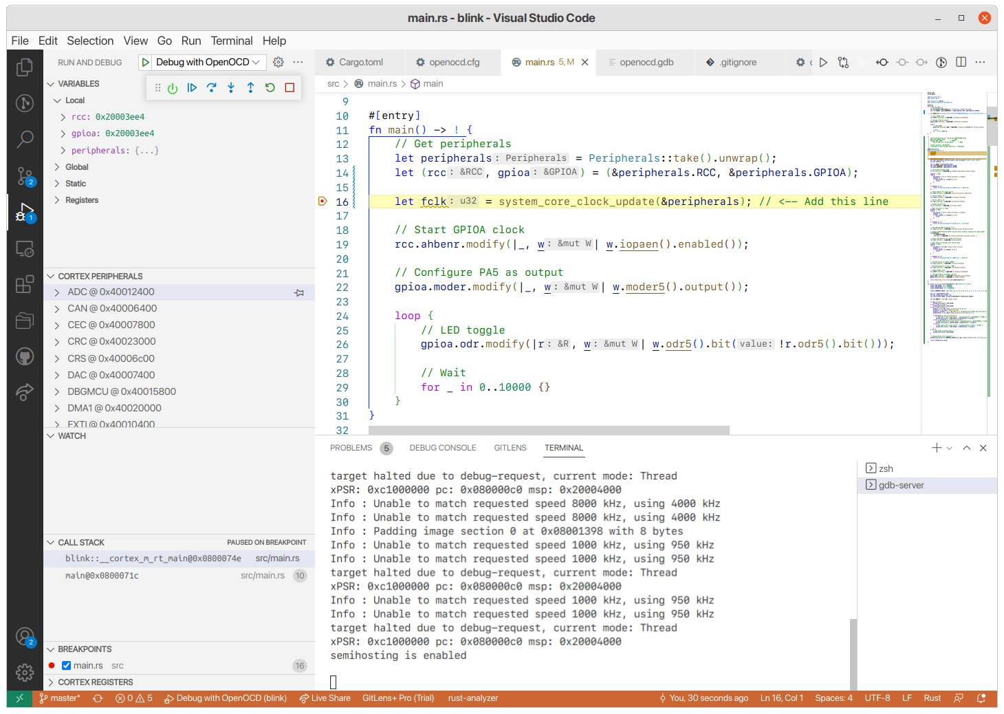
Save the code (Ctrl + S) and start a debug session:

Place a breakpoint on the function call and run the debug to this point:
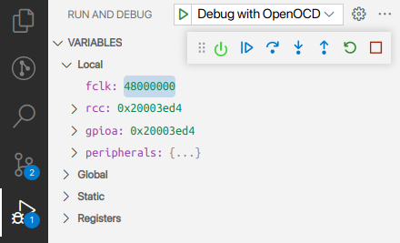
Step over ( ) with the debugger to watch the computed value of
 fclk:
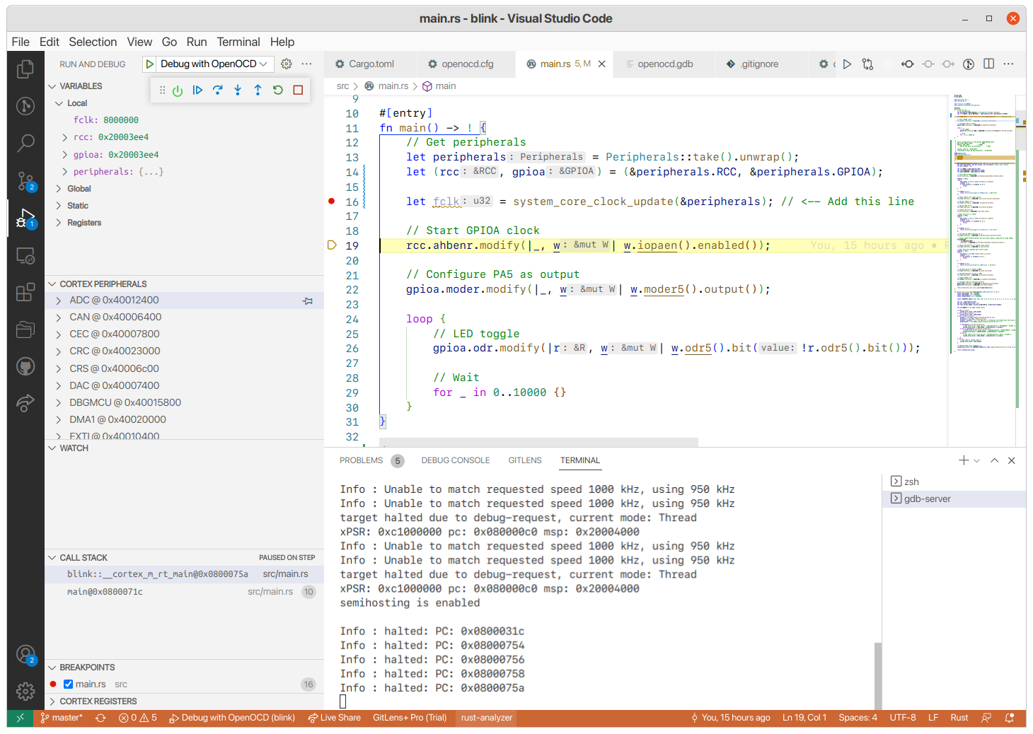
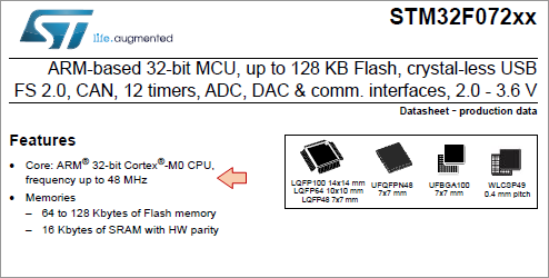
fclk = 8000000, so actual CPU frequency is 8MHz. The device datasheet reveals that STM32F072 runs fine up to 48MHz, so we have room for a 6× faster CPU. How can we do that?
- By understanding the clock scheme of the device.
- By writing a function to configure the clock scheme for 48MHz operation.
3. Understanding the clock scheme
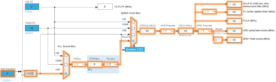
CubeMX provides a handy graphical view of the clock scheme. You can open the first blink project, then open blink.ioc file into the graphical editor and select the Clock Configuration tab.
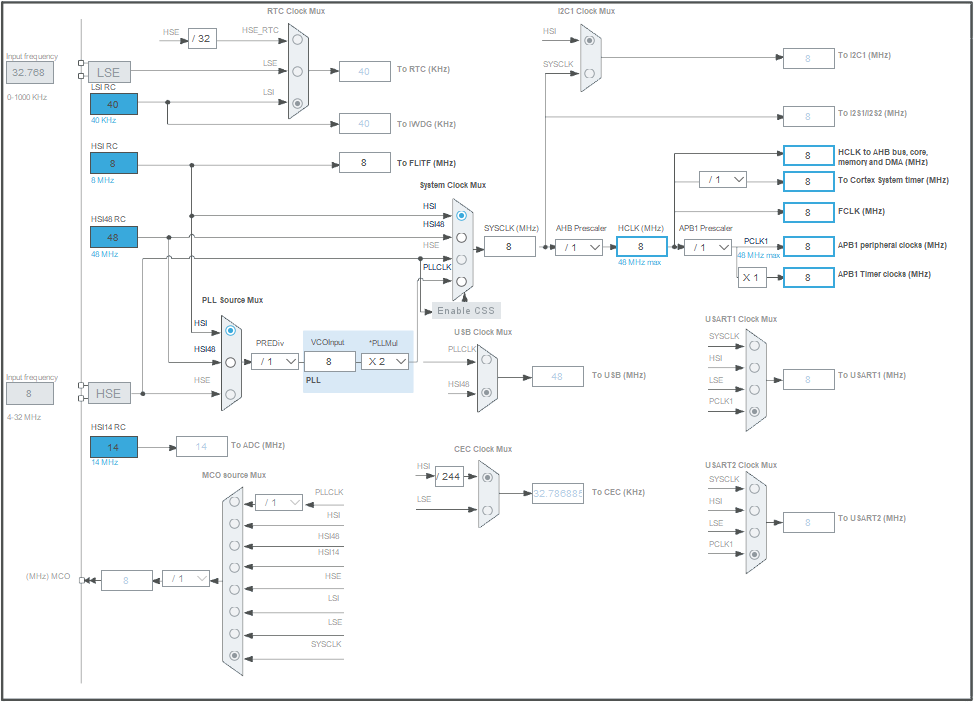
The above picture represents the full hardware architecture of the MCU internal clock system. We find:
- Internal clock sources (RC oscillators) → Available at no additional costs, but neither very precise, nor very stable across the temperature range
- High Speed : HSI, HSI48, HSI14 → default RC-based oscillator for CPU and peripherals.
- Low Speed : LSI → always used with the watchdog timer.
- Inputs for external clock sources (Crystal oscillators) → Required if clock precision and stability are required
- High Speed : HSE → the de facto input for high-speed crystal-based oscillator for CPU and peripherals fast and stable clocking.
- Low Speed : LSE → mostly used with RTC.
- Multiplexers for clock routing (one input among n is connected to the output)
- Frequency dividers (prescalers)
- Frequency multiplier (PLL)
By fine tuning all these boxes, you can achieve a large amount of different clock configurations. Why is it that complex? Because clock and power consumption are tightly linked, and you want the most of the MCU, with as low current as possible. Hence, in power-aware embedded systems, a general rule is:
- Only clock the hardware your application needs
- Lower the clock frequency as much as you can
- Use Low-Power modes (sleep, stop, standby) whenever you can
4. Understanding the default configuration
The 8MHz we observe for the system core clock comes from the default clock configuration at startup (reset state), which in turn is a consequence of the registers that configure the above clock scheme reset states . These registers are part of the RCC (Reset & Clock Control) peripheral. Refer to the the Reference Manual to fully understand the table below.
| RESET STATE | BITS | EFFECT | ||
|---|---|---|---|---|
RCC_CR |
0x0000 XX83 |
HSI ON = 1HSI RDY = 1HSI TRIM = 16 |
The HSI oscillator is ON and ready, with the trimmer set to 8MHz. HSE and PLL are OFF |
|
RCC_CFGR |
0x0000 0000 |
SW = 0HPRE = 0PPRE = 0 |
The HSI input is selected at the System Clock Mux input. SYSCLK = 8MHz. AHB Prescaler and APB Prescaler are set to /1, therefore : - HCLK = 8MHz - PCLK = 8MHz → all peripherals receive a 8MHz clock. |
|
The corresponding path is highlighted below. This is the configuration you have if you do nothing.
5. Writing a new configuration function
Assume we want to push the processor to its 48MHz limit, and then use HSE as the clock source for more stability.
The HSE hardware supports two different configurations (modes):
-
The Oscillator Mode: In this mode, HSE is connected to a crystal/capacitor network. HSE drives this network (unstable closed-loop amplifier) in order to produce oscillations
-
The Bypass Mode: In this mode, HSE receives a clock from an external source on the board. HSE does nothing but letting that clock passing through it.
Then looking at the board schematics, we see that the 2 options have been anticipated on the PCB. We can either use:
- the X3/C33/C34 network with HSE in Oscillator Mode
- or the ST-Link MCO clock source with HSE in Bypass Mode
But looking closer on the board itself, you will see that X3/C33/C34 and R35, R37 are not actually fitted. Footprints are there, but if you want it, you have to buy the parts and then find a soldering iron...
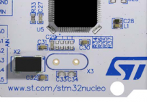
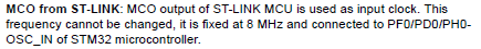
So we're left with the second option, i.e. using the ST-Link MCO (Master Clock Output) as our HSE source, with HSE in Bypass Mode. The User Manual also states that ST-Link MCO is a fixed 8MHz frequency clock.
As we want to achieve a 48MHz CPU clock frequency from the 8MHz external clock source, we need something that multiplies frequencies. This is the purpose of the PLL (Phase Locked Loop) circuit. Using a ×6 multiplication factor within the PLL, we can obtain the targeted 48MHz for the CPU and peripherals.
In summary, the configuration we need to implement is:
Practically, this will be achieved by writing a function that does (in this order):
- Enable HSE in Bypass Mode and make sure it is READY (should already be)
- Choose HSE as the selected input on the PLL Source Mux
- Set the PLL prescaler PREDiv to /1 and the multiplication factor PLLMul to ×6
- Start the PLL and make sure it is READY
- Make sure AHB Prescaler and APB Prescaler are set such that system (CPU & peripherals) will cope with the new frequency
- Switch the System Clock Mux input, from HSI to PLLCLK → At this moment only will the system clock get boosted.
6. Let's boost the system
Using the blink project, open main.rs in the editor. Copy/paste the following function below the main() function. Comments should help you understand what the code does but basically, it just sets the RCC peripheral as above discussed.
In addition, it sets PA8 pin as MCO (Master Clock Output). This is not mandatory. It only provides a convenient way to measure the internal clock frequency with an oscilloscope. Yet, in order to cope with oscilloscopes bandwidth, the 48MHz is divided by /16 so that MCO pin actually exhibits a 3MHz square signal.
/*
 *  Clock configuration for the Nucleo STM32F072RB board
 *  HSE input Bypass Mode    -> 8MHz
 *  SYSCLK, AHB, APB1    -> 48MHz
 *   PA8 as MCO with /16 prescaler   -> 3MHz
 *
 *  Laurent Latorre - 05/08/2017
 *  Translated to Rust by Paul Delestrac - 15/04/2022
 */
#[derive(Debug)]
enum ClockConfigError {
    HSEError,
    PLLError,
    SWError,
}

fn system_clock_config(peripherals: &Peripherals) -> Result<u32, ClockConfigError> {
    let (mut hse_status, mut pll_status, mut sw_status): (bool, bool, bool);
    let mut timeout: i32;

    let rcc = &peripherals.RCC;
    let flash = &peripherals.FLASH;
    let gpioa = &peripherals.GPIOA;

    // Start HSE in Bypass Mode
    rcc.cr.modify(|_, w| w.hsebyp().bypassed().hseon().on());

    timeout = 1000;
    loop {
        hse_status = rcc.cr.read().hserdy().is_ready();
        timeout -= 1;
        if (hse_status) || (timeout <= 0) {
            break;
        };
    }

    if timeout == 0 {
        return Err(ClockConfigError::HSEError); // HSE Error
    };

    // Select HSE as PLL input source
    rcc.cfgr.modify(|_, w| w.pllsrc().hse_div_prediv());

    // Set PLL Prediv to /1
    rcc.cfgr2.modify(|_, w| w.prediv().div1());

    // Set PLL MUL to x6
    rcc.cfgr.modify(|_, w| w.pllmul().mul6());

    // Enable the main PLL
    rcc.cr.modify(|_, w| w.pllon().on());

    // Wait until PLL is ready
    timeout = 1000;
    loop {
        pll_status = rcc.cr.read().pllrdy().is_ready();
        timeout -= 1;
        if (pll_status) || (timeout <= 0) {
            break;
        };
    }

    if timeout == 0 {
        return Err(ClockConfigError::PLLError); // PLL Error
    };

    // Set AHB and APB1 prescaler to /1
    rcc.cfgr.modify(|_, w| w.hpre().div1().ppre().div1());

    // Enable FLASH Prefetch Buffer and set Flash Latency (required for high speed)
    flash
        .acr
        .modify(|_, w| w.prftbe().enabled().latency().ws1());

    // Select the main PLL as system clock source
    rcc.cfgr.modify(|_, w| w.sw().pll());

    // Wait until PLL becomes main switch input
    timeout = 1000;
    loop {
        sw_status = rcc.cfgr.read().sws().is_pll();
        timeout -= 1;
        if (sw_status) || (timeout <= 0) {
            break;
        }
    }

    if timeout == 0 {
        return Err(ClockConfigError::SWError); // SW Error
    }

    // Set MCO source as SYSCLK (48MHz)
    rcc.cfgr.modify(|_, w| w.mco().sysclk());

    // Set MCO prescaler to /16 -> 3MHz
    rcc.cfgr.modify(|_, w| w.mcopre().div16());

    // Enable GPIOA clock
    rcc.ahbenr.modify(|_, w| w.iopaen().enabled());

    // Configure PA8 as alternate function
    gpioa.moder.modify(|_, w| w.moder8().alternate());
    gpioa.afrh.modify(|_, w| w.afrh8().af0());

    return Ok(system_core_clock_update(&peripherals));
}
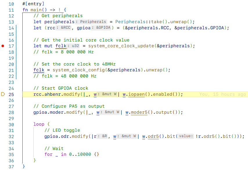
Insert a call to this function at the beginning of main():
#[entry]
fn main() -> ! {
    // Get peripherals
    let peripherals = Peripherals::take().unwrap();
    let (rcc, gpioa) = (&peripherals.RCC, &peripherals.GPIOA);

    // Get the initial core clock value
    let mut fclk = system_core_clock_update(&peripherals);
    // fclk = 8 000 000 Hz

    // Set the core clock to 48MHz
    fclk = system_clock_config(&peripherals).unwrap();
    // fclk = 48 000 000 Hz

    // Start GPIOA clock
    rcc.ahbenr.modify(|_, w| w.iopaen().enabled());

    // Configure PA5 as output
    gpioa.moder.modify(|_, w| w.moder5().output());

    loop {
        // LED toggle
        gpioa.odr.modify(|r, w| w.odr5().bit(!r.odr5().bit()));

        // Wait
        for _ in 0..10000 {}
    }
}
Save the code (Ctrl + S) and start a debug session:
At the beginning of main(), the fclk variable should still be 8000000 (8MHz). Then step over () the system_clock_config() function and watch the fclk value.
The fclk variable should be now 48000000 (48MHz). Well done!
Run ( ) the program and watch the LED... blinking has become pretty nervous, hasn't it?
Probe PA8 pin with an oscilloscope. You should see a 3MHz clock (as a result of 48MHz /16):
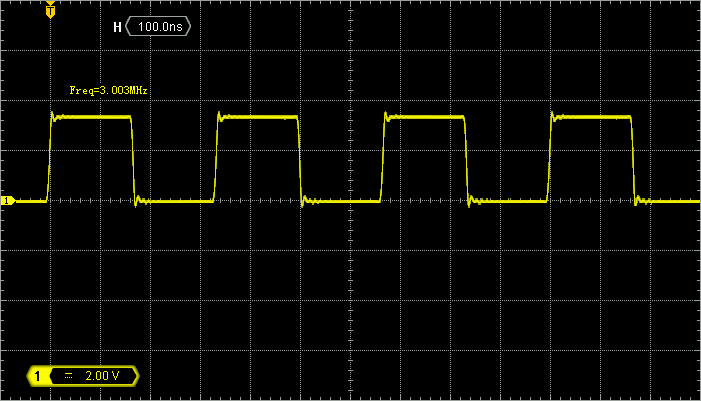
Then suspend the execution ( ) and keep probing PA8. What do you see? Can you explain?
You can terminate ( ) the debug session.
7. Summary
In this tutorial, we introduced the clock setup in the STM32. User settings define clock frequencies for the CPU and for the various peripherals (buses). This is a matter of primary importance:
- You can't configure peripherals, especially timers and communication peripherals if you don't know what is their clock frequency.
- The clock frequency can be changed on-the-fly, depending on the application requirements or the available power at a given moment.
- As you can see, there are several clock domains in the MCU. Fine tuning each domain to the minimum required frequency, at every moment of the application life, is a key for power savings.
At this moment, we tuned clock for maximum operating frequency. Therefore, we considered the performance before the power consumption. All along the subsequent tutorials, we will assume that performance is the priority and keep using that clock configuration, but keep in mind that it is not power friendly. A good approach would be to start a development at maximum speed, then measure what is really needed for the application to perform flawlessly, and finally to reduce the frequency to what is just needed.