
1. Introduction
Analog to Digital Converters (ADC) are involved in several embedded projects. From the capture of UI potentiometers to digitalization of sensor data, the use of ADC is manifest in number of cases. STM32 may have one or more ADCs. An ADC is a complex hardware, that takes room on silicon and that requires power to operate. Therefore, few ADCs are usually embedded in a MCU. In order to achieve conversions on several channels (pins), a single ADC input is connected to one among multiples input pins using a multiplexer. ADCs peripherals can operate on a single channel or on multiples channels sequentially. You can perform a single conversion on demand (or a single sequence), or let ADC work continuously. In this tutorial, you will setup ADC to work continuously on a single channel. If you understand what’s done here, you will be able to adapt the configuration to your needs.
2. Pin mapping
Not any MCU pin can be elected for ADC conversion. You need to refer to the datasheet to discover which pins are connected to ADC input mux.
Note that ADC connection is not considered as an Alternate Function, as we saw for USART pins. ST calls this an Additional Function instead. It is reported in the pin definitions tables of the datasheet.
For example, PA0 and PA1 are connected to ADC input 0 and 1 respectively:
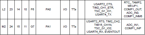
In the STM32F072RB device, there is only one ADC, but the input mux features 16 inputs (0 to 15). There is no reason to prefer a channel among others, unless you have pin restrictions. In the lab, let us arbitrarily choose the ADC channel 11. According to the table below, channel 11 is connected to pin PC1.
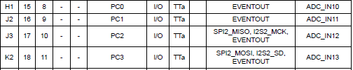
Ultimately, you have the make sure that PC1 is not involved in some board-level function (such as LED, button, USB…). The best source of information is the board schematics. Here, we can see that PC1 is totally free for our purpose.
3. ADC configuration and test
The code below sets the ADC for a single continuous conversion on channel 11. As usual, the first step is to configure associated GPIO in the correct mode (analog here). Next, ADC clock is enabled, followed by ADC registers settings. Refer to the reference manual to grasp a complete understanding of what is done there.
Add the following code to existing src/bsp.rs file in your project:
Now it is time to test this:
/*
 * bps_adc_init()
 * Initialize ADC for a single channel conversion
 * on channel 11 -> pin PC1
 */

pub fn bps_adc_init(peripherals: &Peripherals) {
    let (rcc, gpioc, adc) = (&peripherals.RCC, &peripherals.GPIOC, &peripherals.ADC);

    // Enable GPIOC clock
    rcc.ahbenr.modify(|_, w| w.iopcen().enabled());

    // Configure pin PC1 as analog
    gpioc.moder.modify(|_, w| w.moder1().analog());

    // Enable ADC clock
    rcc.apb2enr.modify(|_, w| w.adcen().enabled());

    // Reset ADC configuration
    adc.cr.reset();
    adc.cfgr1.reset();
    adc.cfgr2.reset();
    adc.chselr.reset();

    // Enable continuous conversion mode
    // and 12-bit resolution
    adc.cfgr1
        .modify(|_, w| w.cont().continuous().res().twelve_bit());

    // Select PCLK/2 as ADC clock
    adc.cfgr2.modify(|_, w| w.ckmode().pclk_div2());

    // Set sampling time to 28.5 ADC clock cycles
    adc.smpr.modify(|_, w| w.smp().cycles28_5());

    // Select channel 11
    //  ADC1->CHSELR |= ADC_CHSELR_CHSEL11;
    adc.chselr.modify(|_, w| w.chsel11().selected());

    // Enable ADC and Start conversion
    adc.cr
        .modify(|_, w| w.aden().enabled().adstart().start_conversion());
}
Now it is time to test this by changing our main function:
#[entry]
fn main() -> ! {
    // Get peripherals
    let peripherals = Peripherals::take().unwrap();
    let adc = &peripherals.ADC;

    // Configure System Clock
    let _fclk = system_clock_config(&peripherals).unwrap();

    // Initialize Debug Console
    let mut console = bsp::bsp_console_init(&peripherals);
    print!(console, "Console ready!\r\n");

    // Initialize and start ADC on PC1
    bsp::bps_adc_init(&peripherals);
    print!(console, "ADC ready!\r\n");

    // Main loop
    loop {
        while adc.isr.read().eoc().bit_is_clear() {}

        print!(console, "ADC value = {}\r\n", adc.dr.read().data().bits());

        for _ in 0..500000 {}
    }
}
ADC conversion result is available in the Data Register (DR). It is a good idea to make sure that last conversion is done before reading this register. This is achieved by polling the EOC (End Of Conversion) flag of ADC1 peripheral.
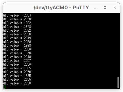
Save the code (Ctrl + S) and start a debug session. Because nothing is actually connected to pin PC1, the conversion result is meaningless. You might have a value representing a voltage close to VCC/2 over 10-bit = 2048.
Note that you could as well use the debugger to monitor ADC results, but in a less “real-time” fashion. To further test the code, one should cook a little bit of hardware.
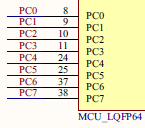
First, locate the PC1 pin on the Nucleo board header:
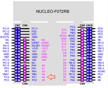
PC1 corresponds to the A4 “Arduino” pin. Leaving PC1 floating may produce random conversion results. Connecting PC1 to GND should display 0 for the ADC value. Connecting PC1 to the +3.3V pin should display something close to 4095 (0x0FFF, the full range for a 12-bit value).
If these simple tests succeed, then it seems that everything is working fine.
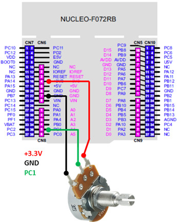
To modulate the ADC input continuously, you can wire a potentiometer this way:
4. Summary
In this tutorial, you have setup ADC for a single channel continuous conversion and used the print in console as a monitor.