
1. Introduction
The Serial Peripheral Interface (SPI) is a synchronous serial communication interface specification used for short-distance communication, primarily in embedded systems. The interface was developed by Motorola in the mid-1980s and has become a de facto standard. Typical applications include Secure Digital cards and liquid crystal displays. SPI devices communicate in full duplex mode using a master-slave architecture with a single master. The master device originates the frame for reading and writing. Multiple slave-devices are supported through selection with individual slave select (SS) (sometimes called chip select (CS)) lines. (https://en.wikipedia.org/wiki/Serial_Peripheral_Interface)
The screenshot below represents the reading of a 16-bit data from the LPS25H pressure and temperature sensor. As you can see, the transaction is performed with only 3 bytes being involved, corresponding to 24 clock cycles (2 times less than with I2C for the same transaction). The price to pay is that SPI requires more wires between master and slave :
- SCK : the bit clock
- MOSI : Master Out / Slave In, used by the master to send data to the slave
- MISO : Master In / Slave Out, used by the master to receive data from the slave
- CS : Chip Select, driven by the master to select a slave among other sharing the same SCK, MOSI, MISO lines
Compare to I2C, SPI protocol is simpler, and faster. It only requires more I/O on the MCU side.
2. SPI Peripheral Initialisation
The code below is an example of SPI1 peripheral configuration for a master, 8-bit, SPI controller role.
Main concerns when initialising SPI peripherals are:
- Configure pins associated with bus lines (SCK, MISO, MOSI) with correct alternate function
- Make sure SPI mode complies with slave datasheet regarding the sampling clock edge. This is done by tuning CPOL and CPHA configuration bits
- Set the bus speed using the clock prescaler
- For the master mode, disable any hardware management of the NSS (internal CS function)
Add this function to your bsp.c/bsp.h library.
/*
 * BSP_SPI1_Init()
 * Initialize SPI1 peripheral @375kHz
 */
void BSP_SPI1_Init()
{
	// SPI_SCK  -> PB3 (AF0)
	// SPI_MISO -> PB4 (AF0)
	// SPI_MOSI -> PB5 (AF0)
	// CS pin	-> PC7 (GPIO)

	// Configure PC7 as CS pin

	// Enable GPIOC clock
	RCC->AHBENR |= RCC_AHBENR_GPIOCEN;

	// Configure PC7 as output
	GPIOC->MODER &= ~GPIO_MODER_MODER7_Msk;
	GPIOC->MODER |= (0x01 <<GPIO_MODER_MODER7_Pos);

	// Configure PC7 as Push-Pull output
	GPIOC->OTYPER &= ~GPIO_OTYPER_OT_7;

	// Configure PC7 as High-Speed Output
	GPIOC->OSPEEDR &= ~GPIO_OSPEEDR_OSPEEDR7_Msk;
	GPIOC->OSPEEDR |= (0x03 <<GPIO_OSPEEDR_OSPEEDR7_Pos);

	// Disable PC7 Pull-up/Pull-down
	GPIOC->PUPDR &= ~GPIO_PUPDR_PUPDR7_Msk;

	// Idle state is high
	GPIOC->BSRR = GPIO_BSRR_BS_7;

	// Configure PB3, PB5, PB5 as SPI1 pins (AF0)

	// Enable GPIOB clock
	RCC->AHBENR |= RCC_AHBENR_GPIOBEN;

	// Configure PB3, PB4, PB5 as AF mode
	GPIOB->MODER &= ~(GPIO_MODER_MODER3 | GPIO_MODER_MODER4 | GPIO_MODER_MODER5);
	GPIOB->MODER |= (0x02 <<6U) |(0x02 <<8U) |(0x02 <<10U);

	// Connect to SPI1 (AF0)
	GPIOB->AFR[0] &= ~(0x00FFF000);
	GPIOB->AFR[0] |=  (0x00000000);

	// Enable SPI1 Clock
	RCC->APB2ENR |= RCC_APB2ENR_SPI1EN;

	// Configure SPI with default config
	// 4-wire = full-duplex (MISO/MOSI on separated lines)
	// 8-bit, no CRC, MSB first
	// CPHA = 0, CPOL = 0 -> SPI mode 0 (first clock rising edge)
	SPI1->CR1 = 0x0000;
	SPI1->CR2 = 0x0000;

	// Set the baudrate to 48MHz /128 = 375kHz (slow, but easy to debug)
	SPI1->CR1 |= 0x06 <<SPI_CR1_BR_Pos;

	// Set data size to 8-bit
	SPI1->CR2 |= 0x07 <<SPI_CR2_DS_Pos;

	// Set as master (SSI must be high), with software managed NSS
	SPI1->CR1 |= SPI_CR1_MSTR | SPI_CR1_SSI | SPI_CR1_SSM;

	// Enable SPI1
	SPI1->CR1 |= SPI_CR1_SPE;
}
Now try this in the main() function and capture the SPI transaction using 4 oscilloscope channels wired to SCK, MOSI, MISO and CS:
/*
 * Project Entry Point
 */

int main(void)
{
	// Configure System Clock for 48MHz from 8MHz HSE
	SystemClock_Config();

	// Initialize LED and USER Button
	BSP_LED_Init();
	BSP_PB_Init();

	// Initialize Debug Console
	BSP_Console_Init();
	my_printf("\r\nConsole Ready!\r\n");
	my_printf("SYSCLK = %d Hz\r\n", SystemCoreClock);

	// Initialize SPI1
	BSP_SPI1_Init();

	// Try and send something
	SPI1->DR = 0x55;

	while(1)
	{
	}
}
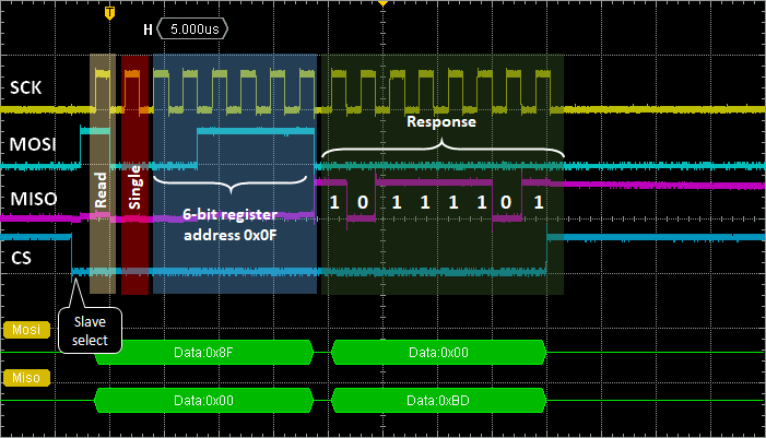
If everything goes well, you'll get this:
The above snapshot confirms:
- that we've suceeded in configuring GPIO alternate functions to work with SPI1
- that writing to the SPI_DR register fires the SPI transaction up
- that clock frequency is as expected (375kHz)
- that the 0x55 byte is well transmitted on MOSI. Note that 0x55 correspond to the 01010101 binary sequence, which is convenient for debug
- that nothing was transmitted by any slave (MISO stays low)
That's a good start. Yet, although we did configure SPI peripheral to work with 8-bit data, one can see that actually 16 clock cycles have been generated after the loading of the SPI_DR register. Why is that?
The reason is stated in page 758 of the reference manual: When the data frame size fits into one byte (less than or equal to 8 bits), data packing is used automatically when any read or write 16-bit access is performed on the SPIx_DR register. The double data frame pattern is handled in parallel in this case. At first, the SPI operates using the pattern stored in the LSB of the accessed word, then with the other half stored in the MSB.
In order to avoid the so-called data packing, one should make sure that only 8-bit access is used when writing to the SPI_DR register.
You can try this:
        // Try and send something
	*(__IO uint8_t *)&SPI1->DR = 0x55;
And you'll get what you want, i.e. a single byte transfer:
If you're curious about the effect of that specific register casting, you'll need to dig into the assembly code. You'll discover that the writing into SPI_DR is done using the SRTB opcode (forcing byte operation), instead of STR opcode in case of regular writing.
|
|
3. Read Transaction
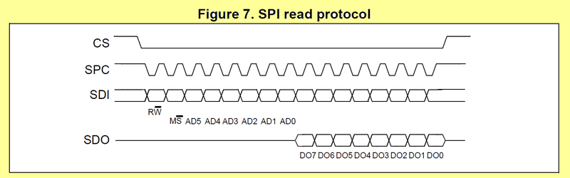
SPI, in full-duplex mode, performs writings (on MOSI) and readings (on MISO) simultaneously every clock edge. Obviously, you first need to tell the slave what operation you want to perform. This is done with the first byte transfer that generally contains fields such as :
- a slave register address (7-bit or less), right aligned
- the nature READ/WRITE of the operation (bit7)
- optional bits depending on slave-specific protocol
Looking at LPS25H datasheet, we can see that:
- register addresses are 6-bit (0-5)
- bit 6 is a MULTIPLE/SINGLE switch indicating whether you want to read/write one or several consecutive registers
- bit 7 is the READ/WRITE switch
Before going any further, again, you'll need to know a little about SPI peripheral flags used to control transactions.
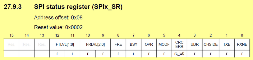
SPI peripheral features 2 FIFO buffers, one for TX, one for RX. These FIFO are 4 bytes deep. Access to the SPI_DR register, actually adds or removes data into/from these FIFOs. The process is transparent, but you need to understand how it works in order to make correct use of status flags. In particular, let us focus on TXE and RXNE flags.
The figure below is a simplified illustration of the SPI behavior. Writing into SPI_DR register puts data to be sent into the TX_FIFO. If it is available (i.e. not currently transmitting), the data is transferred right away into the MOSI shift register, freeing quite instantaneously the TX_FIFO. If the shift register is busy, the data is held into the TX_FIFO (consider this as a waiting queue of data to be sent). If more data are written into SPI_DR, successive TX_FIFO slots are used, up to 4. The TXE (TX Empty) flag signals whether you can add data to the FIFO, or not. It is set when the TX_FIFO is empty, and drops when TX_FIFO reaches half-full (i.e. 2 bytes in the waiting list).
The same thing happens on the receiver side. When a byte is received on the MISO line, it is first put into the RX_FIFO waiting list. You can poll the RXNE (RX Not Empty) flag to know if there is something to gather in the RX_FIFO. Reading the SPI_DR register removes the oldest data from the RX_FIFO waiting list. You can program the RX_FIFO threshold so that RXNE is raised when RX_FIFO contains 1 (FRXTH=1) or 2 (FRXTH=0) bytes.
The easy way to handle SPI transactions, when throughput is not an issue, is to do the following for each single byte to be transferred (to/from) the slave :
- Make sure TXE is set
- Write data to be sent into the SPI_DR register. That will start an 8 clock cycles transaction on both MOSI and MISO
- Wait for RXNE to be set. This will occur after the 8th clock cycle
- Read received data from SPI_DR register
Doing so, you're not taking any benefit from the dual FIFO architecture, but it works. Note that RX FIFO threshold MUST be set to 1-byte, so that RXNE flag is raised as soon as one byte arrives in the RX_FIFO.
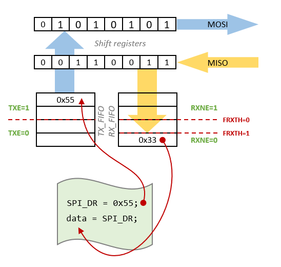
Let us try this approach to read the WHO_AM_I register (address 0x0F) of the LPS25H. The answer should be 0xBD (10111101) according to the device datasheet:
![]()
First, add this function into your bsp.c/bsp.h library. This function just executes the above 4-step sequence. It takes the byte to be sent on MOSI as argument, and returns the byte received on MISO:
uint8_t BSP_SPI_SendReceive(uint8_t tx_byte)
{
	uint8_t	rx_byte;

	// Make sure TXE is set before sending data
	while((SPI1->SR & SPI_SR_TXE_Msk) == 0);

	// Send tx_byte
	*(__IO uint8_t *)&SPI1->DR = tx_byte;

	// Wait until incoming data has arrived
	while((SPI1->SR & SPI_SR_RXNE_Msk) == 0);

	// Read data
	rx_byte = *(__IO uint8_t *)&SPI1->DR;

	return rx_byte;
}
And then, add the code below to the main() function. Note that the transaction must be surrounded by software management of the CS pin.
/*
 * Project Entry Point
 */

int main(void)
{
	uint8_t lps25h_id;

	// Configure System Clock for 48MHz from 8MHz HSE
	SystemClock_Config();

	// Initialize LED and USER Button
	BSP_LED_Init();
	BSP_PB_Init();

	// Initialize Debug Console
	BSP_Console_Init();
	my_printf("\r\nConsole Ready!\r\n");
	my_printf("SYSCLK = %d Hz\r\n", SystemCoreClock);

	// Initialize SPI1
	BSP_SPI1_Init();

	// Set FIFO threshold to 1-byte
	SPI1->CR2 |= SPI_CR2_FRXTH;

	// Select slave (CS -> low)
	GPIOC->BSRR = GPIO_BSRR_BR_7;

	// Send WHO_AM_I register address with READ bit
	BSP_SPI_SendReceive(0x0F | 0x80);

	// Send whatever to generate 8 clock cycles and get the response from slave
	lps25h_id = BSP_SPI_SendReceive(0x00);

	// Release slave (CS -> High)
	GPIOC->BSRR = GPIO_BSRR_BS_7;

	my_printf("LPS25H Device ID = 0x%02x\r\n", lps25h_id);

	while(1)
	{
	}
}
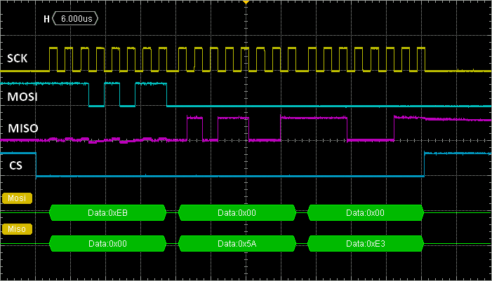
Now you can observe the whole reading transaction:
And the corresponding terminal output:
 |
 Commit name "SPI Read" Commit name "SPI Read" Push onto Gitlab Push onto Gitlab |
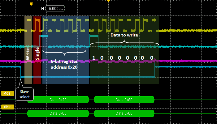
4. Write Transaction
From what we've learned above, the write transaction is quite straightforward. It's almost the same sequence. You only need to change the R/W bit in the first byte, and then transmit the second byte as the data to be written into slave register.
According to the LPS25H datasheet, the device is not active when powered on. In order to turn it into the active mode, one need to set bit 7 (PD) of the CTRL_REG1 register at address 0x20. This is done by writing 0x80 into register at address 0x20.
Try this:
/*
 * Project Entry Point
 */

int main(void)
{
	// Configure System Clock for 48MHz from 8MHz HSE
	SystemClock_Config();

	// Initialize LED and USER Button
	BSP_LED_Init();
	BSP_PB_Init();

	// Initialize Debug Console
	BSP_Console_Init();
	my_printf("\r\nConsole Ready!\r\n");
	my_printf("SYSCLK = %d Hz\r\n", SystemCoreClock);

	// Initialize SPI1
	BSP_SPI1_Init();

	// Set FIFO threshold to 1-byte
	SPI1->CR2 |= SPI_CR2_FRXTH;

	// Select slave (CS -> low)
	GPIOC->BSRR = GPIO_BSRR_BR_7;

	// Send register address to write to
	BSP_SPI_SendReceive(0x20);

	// Send data to write (turn LPS25H on)
	BSP_SPI_SendReceive(0x80);

	// Release slave (CS -> High)
	GPIOC->BSRR = GPIO_BSRR_BS_7;

	while(1)
	{
	}
}
|
Commit name "SPI Write" Push onto Gitlab |
5. Sensor Driver
Based on the above code samples, we can now package LPS25H reading and writing functions into something more user-friendly. Up to now, only one byte was transferred after the register address. In a generic SPI communication, you'll often want to transfer more than one byte. For instance, if the data to read is wider than 8-bit, you'll need to collect multiple bytes.
Access of multiple bytes from SPI devices does not require to send register address for every single byte you want to read or write. You only need to start the transaction with the first (base) address of the register segment you want to access and then, the slave SPI state machine will automatically increment register address after each byte has been accessed. Sometimes this feature is implicit. In the LPS25H, the address auto-increment mechanism must be explicitly turned on by setting the M/S bit (bit-6) within the register address byte.
A generic SPI read function would be more like this:
void BSP_LPS25H_Read(uint8_t register_address, uint8_t *buffer, uint8_t nbytes)
{
	uint8_t		ms_bit_msk;
	uint8_t		n;

	// Set the M/S bit depending on the number of byte to read
	if(nbytes > 1) 	ms_bit_msk = 0x40;    // bit-6 mask
	else		ms_bit_msk = 0x00;

	// Set FIFO threshold to 1-byte
	SPI1->CR2 |= SPI_CR2_FRXTH;

	// Select slave (CS -> low)
	GPIOC->BSRR = GPIO_BSRR_BR_7;

	// Send register address to read from
	BSP_SPI_SendReceive(register_address | 0x80 | ms_bit_msk);

	// Read loop
	n = nbytes;

	while(n>0)
	{
		*buffer = BSP_SPI_SendReceive(0x00);
		buffer++;
		n--;
	}

	// Release slave (CS -> High)
	GPIOC->BSRR = GPIO_BSRR_BS_7;
}
The write function is kept simple, since LPS25H has only 8-bit registers for device configuration, we can work with a simple 2-byte (address/data) protocol:
void BSP_LPS25H_Write(uint8_t register_address, uint8_t data)
{
	// Set FIFO threshold to 1-byte
	SPI1->CR2 |= SPI_CR2_FRXTH;

	// Select slave (CS -> low)
	GPIOC->BSRR = GPIO_BSRR_BR_7;

	// Send register address to write to
	BSP_SPI_SendReceive(register_address);

	// Send data to write
	BSP_SPI_SendReceive(data);

	// Release slave (CS -> High)
	GPIOC->BSRR = GPIO_BSRR_BS_7;
}
And now, we can play with the sensor:
/*
* Project Entry Point
*/
int main(void)
{
uint8_t lps25h_id;
uint8_t spi_buffer[5];
uint32_t pressure;
int16_t temperature;
// Configure System Clock for 48MHz from 8MHz HSE
SystemClock_Config();
// Initialize LED and USER Button
BSP_LED_Init();
BSP_PB_Init();
// Initialize Debug Console
BSP_Console_Init();
my_printf("\r\nConsole Ready!\r\n");
my_printf("SYSCLK = %d Hz\r\n", SystemCoreClock);
// Initialize SPI1
BSP_SPI1_Init();
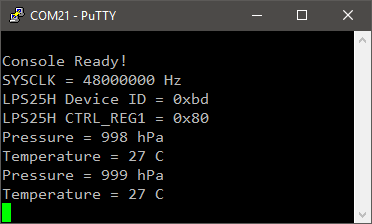
// Read LPS25H device ID
BSP_LPS25H_Read(0x0F, &lps25h_id, 1);
my_printf("LPS25H Device ID = 0x%02x\r\n", lps25h_id);
// Turn LPS25H device ON
BSP_LPS25H_Write(0x20, 0x80);
// Read back CTRL_REG1 register
BSP_LPS25H_Read(0x20, spi_buffer, 1);
my_printf("LPS25H CTRL_REG1 = 0x%02x\r\n", spi_buffer[0]);
// Set averaging to minimum
BSP_LPS25H_Write(0x10, 0x00);
while(1)
{
// Trigger a one-shot pressure measure
BSP_LPS25H_Write(0x21, 0x01);
// Allow some time for sensor to perform
BSP_DELAY_ms(10);
// Read sensor data
// Pressure level in registers 0x2A | 0x29 | 0x28
// Temperature in registers 0x2C | 0x2B
BSP_LPS25H_Read(0x28, spi_buffer, 5);
// Compute pressure
pressure = (uint32_t)( (spi_buffer[2] <<16U) +
(spi_buffer[1] << 8U) +
(spi_buffer[0] << 0U));
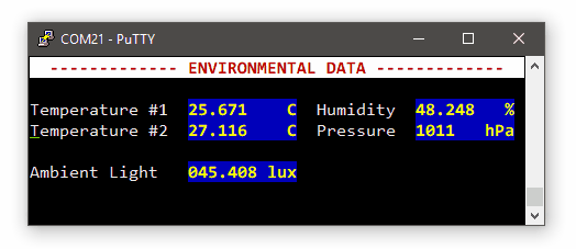
my_printf("Pressure = %d hPa\r\n", pressure / 4096);
// Compute temperature
temperature = (int16_t)((spi_buffer[4] <<8U) + (spi_buffer[3] <<0U));
my_printf("Temperature = %d C\r\n", (uint8_t)(42.5f + ((float)temperature/480.0f)));
BSP_DELAY_ms(1000);
}
}
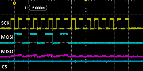
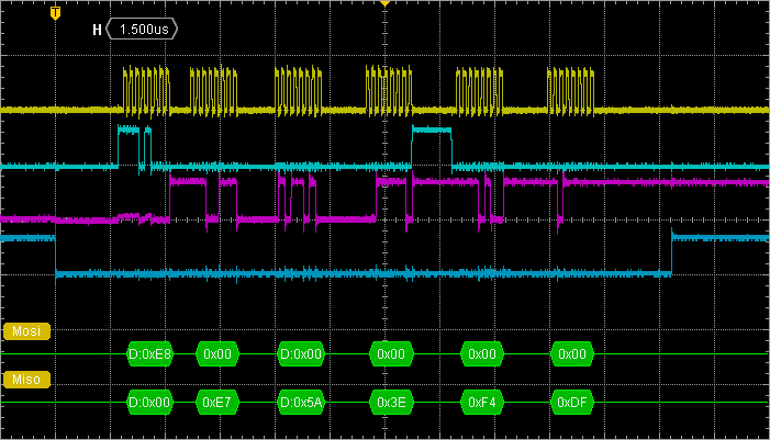
This is a snapshot the the SPI transaction collecting 5 bytes (3 for pressure, 2 for temperature):
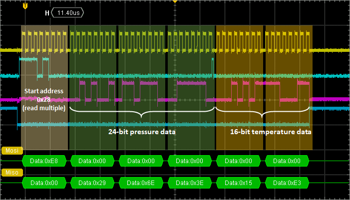
Note that the whole transaction takes about 140µs to complete.
In a lot of situations, the above SPI driver is just fine, and you may be happy with it. Typical situations are the configuration and reading of sensors where the reading of few bytes seldom happen, so that SPI traffic is not very heavy.
In the situation where large amount of data need to be transferred one can make use of SPI FIFOs to speed up things. A good example of heavy traffic in embedded electronic project is the access to SD cards using SPI. Note that SD cards support SPI, but also provide a faster bus called SDIO. SDIO (also called SDMMC) is available on high-end STM32 devices and is a 6-wire bus.
|
Commit name "SPI Sensor driver" Push onto Gitlab |
6. Using FIFOs
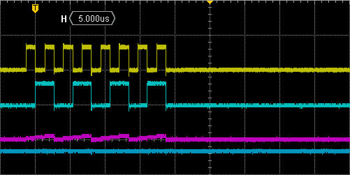
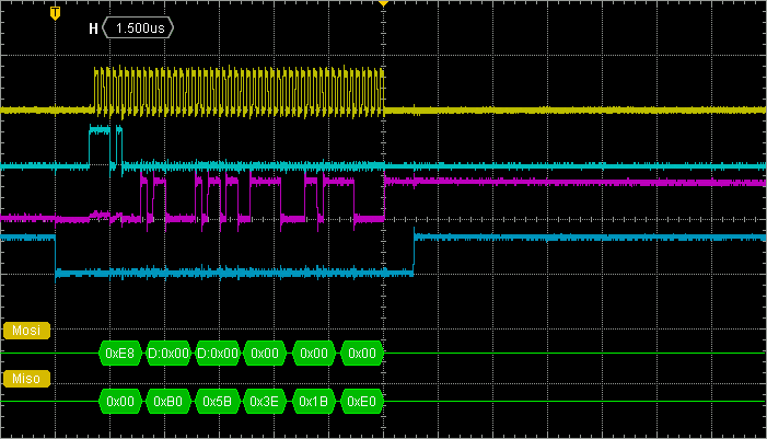
The above approach to deal with SPI flags is perfectly valid, but far from being optimized. You cannot see this at low clock speed, but it becomes obvious if you speed up clock up to 6Mhz. You can do this by changing the baud rate prescaler settings in the BSP_SPI1_Init() function:
	// Set the baudrate to 48MHz /8 = 6MHz
	SPI1->CR1 |= 0x02 <<SPI_CR1_BR_Pos;
Capture the previous SPI transaction again. It is now faster with about 22µs for the whole thing to complete. Yet, you can see that a lot of time is lost between each byte transfer. That's an issue SPI FIFOs should be able to handle.
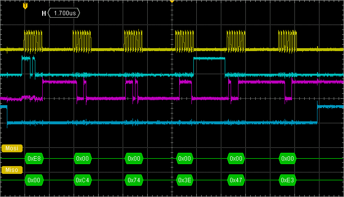
The code below is an attempt to speed up BSP_LPS25H_Read() function. The idea here is to fill TX_FIFO as soon as TXE is set, while reading from RX_FIFO as soon as RXNE is set:
void BSP_LPS25H_ReadFast(uint8_t register_address, uint8_t *buffer, uint8_t nbytes)
{
    uint8_t	ms_bit_msk;
    uint8_t	n_tx, n_rx;

    // Set the M/S bit depending on the number of byte to read
    if(nbytes > 1) 	ms_bit_msk = 0x40;
    else		ms_bit_msk = 0x00;

    // Set FIFO threshold to 1-byte
    SPI1->CR2 |= SPI_CR2_FRXTH;

    // Select slave (CS -> low)
    GPIOC->BSRR = GPIO_BSRR_BR_7;

    n_tx = nbytes + 1;    // Add 1 byte to take register address into account
    n_rx = nbytes + 1;

    while(n_rx>0)
    {
	// Write to TX_FIFO if possible
        if (((SPI1->SR & SPI_SR_TXE_Msk) != 0) & (n_tx > 0))
	{
	    if (n_tx == (nbytes+1))
	    {
		// If this is first byte, send register address
		*(__IO uint8_t *)&SPI1->DR = (register_address | 0x80 | ms_bit_msk);
	    }
	    else
	    {
		// Otherwise send zeros
		*(__IO uint8_t *)&SPI1->DR = 0x00;
	    }
	    n_tx--;
	}

	// Read from RX_FIFO if not empty
	if ((SPI1->SR & SPI_SR_RXNE_Msk) != 0)
	{
	    if (n_rx == (nbytes+1))
	    {
		// Dummy access to SPI_DR (first byte)
		*(__IO uint8_t *)&SPI1->DR;
	    }
	    else
	    {
		// Read from slave
		*buffer = *(__IO uint8_t *)&SPI1->DR;
		buffer++;
	    }
	    n_rx--;
	}
    }

    // Release slave (CS -> High)
    GPIOC->BSRR = GPIO_BSRR_BS_7;
}
In main(), replace BSP_LPS25H_Read() by BSP_LPS25H_ReadFast() when reading the sensor results. Watch how transaction now performs with the oscilloscope:
Surprisingly, the improvement is not that big. We can see that dead times are slightly shorter. Whole transaction now takes 17µs to complete. But still, we were expecting more...
As we're dealing with software handling of data and FIFOs, maybe could we try to involve some degree of compilation optimization. Build the very same program with -O1 optimization level and watch the result:
The clock now runs uninterrupted and the whole transaction takes less than 10µs to complete. Quite good indeed!
Well, you may now argue that calling for compiler optimization is quite an unfair and easy trick. You would be right...
You may also wonder how would have performed the first BSP_LPS25H_Read() function under the same optimization condition. Try for yourself! You'll see that transaction takes about 15µs. That's good, but still below the BSP_LPS25H_ReadFast() performance, and holes in the clock signal are back.
Actually, software management of the FIFOs implies speed limitations. The clean way to get full speed SPI transactions is to rely on hardware data transfer based on DMA. Well, this tutorial is long enough, so let's keep this for another time...
Do not forget to turn optimization level back to -O0 if you keep working on that project, and lower the clock speed for robustness.
Add new comment