
1. Introduction
Analog to Digital Converters (ADC) are involved in several embedded projects. From the capture of UI potentiometers to digitalization of sensor data, the use of ADC is manifest in number of cases. STM32 may have one or more ADCs. An ADC is a complex hardware, that takes room on silicon and that requires power to operate. Therefore, few ADCs are usually embedded in a MCU. In order to achieve conversions on several channels (pins), a single ADC input is connected to one among multiples input pins using a multiplexer. ADCs peripherals can operate on a single channel or on multiples channels sequentially. You can perform a single conversion on demand (or a single sequence), or let ADC work continuously. In this tutorial, you will setup ADC to work continuously on a single channel. If you understand what’s done here, you will be able to adapt the configuration to your needs.
2. Pin mapping
Not any MCU pin can be elected for ADC conversion. You need to refer to the datasheet to discover which pins are connected to ADC input mux.
Note that ADC connection is not considered as an Alternate Function, as we saw for USART pins. ST calls this an Additional Function instead. It is reported in the pin definitions tables of the datasheet.
For example, PA0 and PA1 are connected to ADC input 0 and 1 respectively:
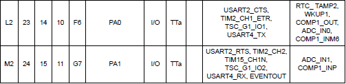
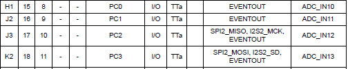
In the STM32F072RB device, there is only one ADC, but the input mux features 16 inputs (0 to 15). There is no reason to prefer a channel among others, unless you have pin restrictions. In the lab, let us arbitrarily choose the ADC channel 11. According to the table below, channel 11 is connected to pin PC1.
Ultimately, you have the make sure that PC1 is not involved in some board-level function (such as LED, button, USB…). The best source of information is the board schematics. Here, we can see that PC1 is totally free for our purpose.
3. ADC configuration and test
The code below sets the ADC for a single continuous conversion on channel 11. As usual, the first step is to configure associated GPIO in the correct mode (analog here). Next, ADC clock is enabled, followed by ADC registers settings. Refer to the reference manual to grasp a complete understanding of what is done there.
Add the following code to existing bsp.c file in the my_project project:
/*
 * ADC_Init()
 * Initialize ADC for a single channel conversion
 * on channel 11 -> pin PC1
 */

void BSP_ADC_Init()
{
	// Enable GPIOC clock
	RCC->AHBENR |= RCC_AHBENR_GPIOCEN;

	// Configure pin PC1 as analog
	GPIOC->MODER &= ~GPIO_MODER_MODER1_Msk;
	GPIOC->MODER |= (0x03 <<GPIO_MODER_MODER1_Pos);

	// Enable ADC clock
	RCC->APB2ENR |= RCC_APB2ENR_ADC1EN;

	// Reset ADC configuration
	ADC1->CR 	= 0x00000000;
	ADC1->CFGR1  = 0x00000000;
	ADC1->CFGR2  = 0x00000000;
	ADC1->CHSELR = 0x00000000;

	// Enable continuous conversion mode
	ADC1->CFGR1 |= ADC_CFGR1_CONT;

	// 12-bit resolution
	ADC1->CFGR1 |= (0x00 <<ADC_CFGR1_RES_Pos);

	// Select PCLK/2 as ADC clock
	ADC1->CFGR2 |= (0x01 <<ADC_CFGR2_CKMODE_Pos);

	// Set sampling time to 28.5 ADC clock cycles
	ADC1->SMPR = 0x03;

	// Select channel 11
	ADC1->CHSELR |= ADC_CHSELR_CHSEL11;

	// Enable ADC
	ADC1->CR |= ADC_CR_ADEN;

	// Start conversion
	ADC1->CR |= ADC_CR_ADSTART;
}
Add the prototype declaration to bsp.h:
/*
 * ADC functions
 */

void BSP_ADC_Init		(void);
Now it is time to test this:
// Main program

int main()
{
	uint32_t	i;

	// Configure System Clock
	SystemClock_Config();

	// Initialize Debug Console
	BSP_Console_Init();
	my_printf("Console ready!\r\n");

	// Initialize and start ADC on PC1
	BSP_ADC_Init();
	my_printf("ADC ready!\r\n");

	// Main loop
	while(1)
	{
		// Wait here until ADC EOC
		while ((ADC1->ISR & ADC_ISR_EOC) != ADC_ISR_EOC);

		// Report result to console
		my_printf("ADC value = %d\r\n", ADC1->DR);

		// Wait about 200ms
		for (i=0; i<500000; i++);
	}
}
ADC conversion result is available in the Data Register (DR). It is a good idea to make sure that last conversion is done before reading this register. This is achieved by polling the EOC (End Of Conversion) flag of ADC1 peripheral.
Save all ![]() , build
, build ![]() and run
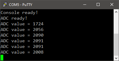
and run ![]() . Because nothing is actually connected to pin PC1, the conversion result is meaningless. You might have a value representing a voltage close to VCC/2 over 10-bit = 2048.
. Because nothing is actually connected to pin PC1, the conversion result is meaningless. You might have a value representing a voltage close to VCC/2 over 10-bit = 2048.
 |
 Commit name "ADC driver" Commit name "ADC driver" Push onto Gitlab Push onto Gitlab |
Note that you could as well use the debugger to monitor ADC results, but in a less “real-time” fashion. To further test the code, one should cook a little bit of hardware.
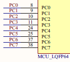
First, locate the PC1 pin on the Nucleo board header:
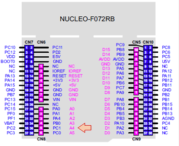
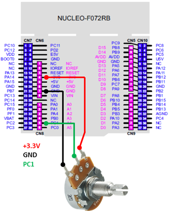
PC1 corresponds to the A4 “Arduino” pin. Leaving PC1 floating may produce random conversion results. Connecting PC1 to GND should display 0 for the ADC value. Connecting PC1 to the +3.3V pin should display something close to 4095 (0x0FFF, the full range for a 12-bit value).
If these simple tests succeed, then it seems that everything is working fine.
To modulate the ADC input continuously, you can wire a potentiometer this way:
4. Monitoring with STM32CubeMonitor
4.1. Code preparation
Because we can only monitor global variables, let’s add a global variable to store ADC result, and shorten the delay a little:
// GLobal variables

uint16_t	ADC_result;

// Main program

int main()
{
	uint32_t	i;

	// Configure System Clock
	SystemClock_Config();

	// Initialize Debug Console
	BSP_Console_Init();
	my_printf("Console ready!\r\n");

	// Initialize and start ADC on PC1
	BSP_ADC_Init();
	my_printf("ADC ready!\r\n");

	// Main loop
	while(1)
	{
		// Wait here until ADC EOC
		while ((ADC1->ISR & ADC_ISR_EOC) != ADC_ISR_EOC);

		// Report result to console
		ADC_result = ADC1->DR;
		my_printf("ADC value = %d\r\n", ADC_result);

		// Wait about 40ms
		for (i=0; i<100000; i++);
	}
}
Save ![]() and build
and build ![]() the project. Verify that you have no errors or warning
the project. Verify that you have no errors or warning
Then flash ![]() your target board . Check in your terminal that the program is working well, just as before but with faster sampling.
your target board . Check in your terminal that the program is working well, just as before but with faster sampling.
4.2. STM32CubeMonitor setup
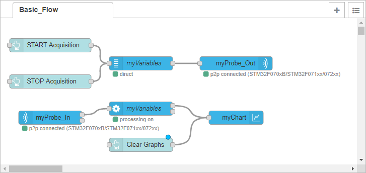
Start STM32CubeMonitor application from Windows start menu. We will start with the basic flow template shown below. It has everything we need to monitor our ADC conversion result.
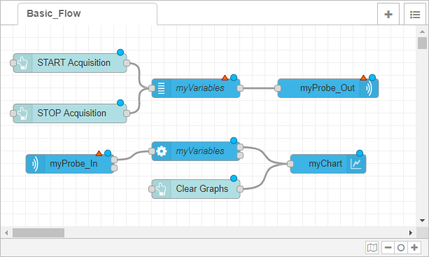
We need to configure some boxes. Double-click the ![]() block.
block.
We have to tell the monitor which executable file contains the variables list we want to monitor. Click the ![]() button.
button.
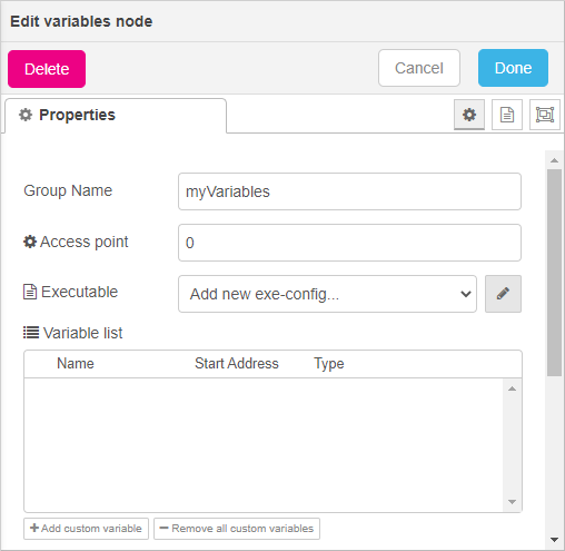
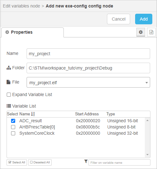
In the next form, fill in the Name and Folder fields. The folder is your project \Debug folder, which contains the my_project.elf executable file. When completed, the software should display the my_project.elf file using the File dropdown list. When selected, the Variable List updates and let you choose which variables you want to monitor. Just select ADC_result.
When done, click ![]() .
.
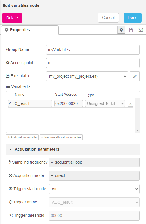
The Edit variables node form updates and the Variable list is now populated with the variables you've selected for monitoring. You can further set Acquisition parameters. Here we choose to sample data as fast as possible (sequential loop).
Click ![]() .
.
Double-click the ![]() block.
block.
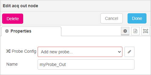
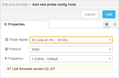
Click the Probe Config edit button ![]() . Use Probe Name the dropdown list to find and select your ST-Link device (make sure your Nucleo is connected, and that no debug session is running in STM32CubeIDE). It should be listed here.
. Use Probe Name the dropdown list to find and select your ST-Link device (make sure your Nucleo is connected, and that no debug session is running in STM32CubeIDE). It should be listed here.
When done, click ![]() . In the Edit acq out node, review the settings. You can use the
. In the Edit acq out node, review the settings. You can use the ![]() button to get your Nucleo ST-Link LED blinking. That can be useful when using multiple ST-Link probes.
button to get your Nucleo ST-Link LED blinking. That can be useful when using multiple ST-Link probes.

Click ![]() .
.
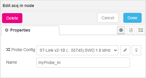
Double-click the ![]() block. In the Probe Config field, select your ST-Link device.
block. In the Probe Config field, select your ST-Link device.
Click ![]() .
.
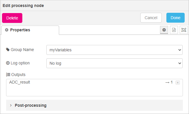
Double-click the ![]() block. Review the settings. Note that ADC_result is routed to output #1 which is connected to the Chart block in the flow chart.
block. Review the settings. Note that ADC_result is routed to output #1 which is connected to the Chart block in the flow chart.
Click ![]() .
.
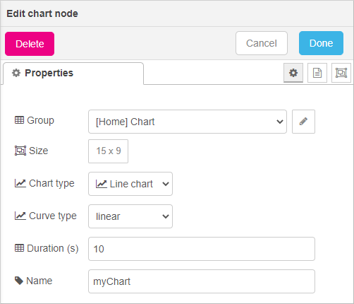
Finally double-click the ![]() and review the settings.
and review the settings.
Click ![]() .
.
4.3. Start the Dashboard
The flow is now fully set. Click the ![]() button and watch for messages:
button and watch for messages:

Looking at the flow chart, the different nodes display a status signaling that connection and processing is now effective.
Start the dashboard by clicking ![]()
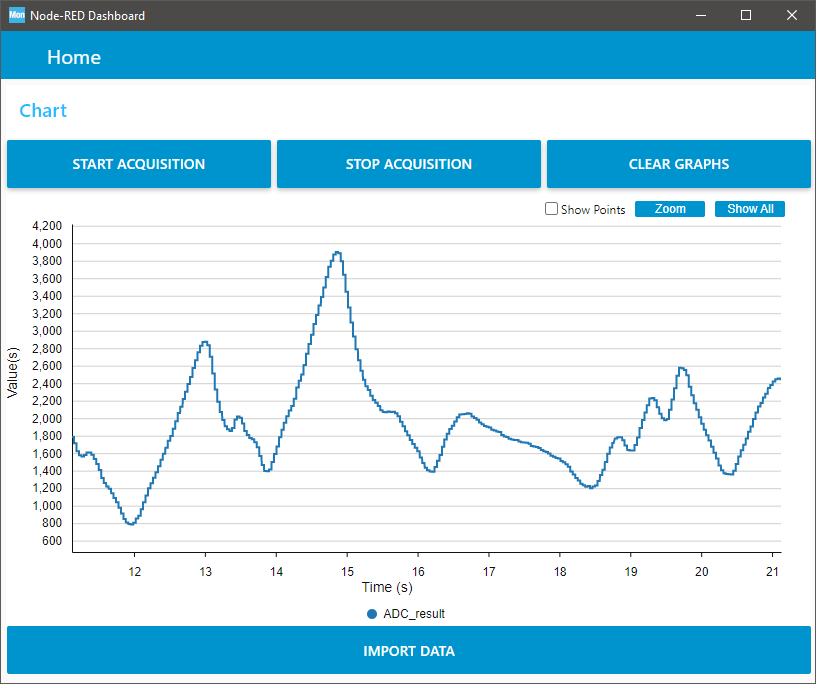
Then play with the upper buttons (START Acquisition / STOP Acquisition) and the potentiometer attached to ADC channel. You can live-monitor the result of ADC conversion, that is to say, you can now monitor the fluctuations of the voltage applied on PC1 pin, just like with an oscilloscope.
Make sure you stop the acquisition before you leave the dashboard otherwise you may not be able to access the ST-Link from STM32CubeIDE unless you unplug/plug the Nucleo board.
5. Summary
In this tutorial, you have setup ADC for a single channel continuous conversion and make use of STM32CubeMonitor to real-time monitor the conversion result.
Add new comment