
1. Introduction

I²C (Inter-Integrated Circuit), pronounced I-squared-C, is a synchronous, multi-master, multi-slave, packet switched, single-ended, serial computer bus invented in 1982 by Philips Semiconductors (now NXP Semiconductors). It is widely used for attaching lower-speed peripheral ICs to processors and microcontrollers in short-distance, intra-board communication. Alternatively I²C is spelled I2C (pronounced I-two-C) or IIC (pronounced I-I-C). (https://en.wikipedia.org/wiki/I%C2%B2C)
I2C is a 2-wire bus (3 actually, if you consider GND) :
- One for a clock → SCL
- One for the data → SDA
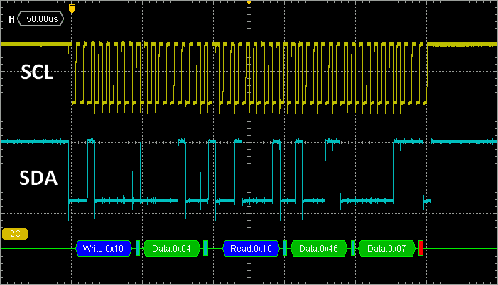
Before going into any detail, just take a look at the screenshot below, representing the STM32 reading a 16-bit result from an ambient light sensor. As you may already notice, the process is not quite straightforward... The expected data is found around the end of the transaction (0x0746) representing some units of light (lux). Nearly 50 clock cycles have been required for the whole transfer. That's 500µs considering a clock frequency of 100kHz.
A single I2C transaction involves one master device and one slave device. In the following, the master device is the microcontroller, and the slave is an external sensor. Both can take control over the SDA line, but not at the same time. SCL is always driven by the master.
Because both master and slave may take control over the SDA line, there could be a risk of conflictual situations where both are trying to pull or push opposite levels at the same time. Such case would lead to severe damage of the weakest side. That risk is eliminated by using open-drain outputs for any SCL and SDA lines on the I2C bus. The logic '1' is therefore achieved by external pull-up resistors. '1' is the default state, when no device is pulling a zero on the bus. '0' always wins, if at least one device says so.
You may have a look at the I2C-bus specification and user manual (Rev. 6 — 4 April 2014). It's only 64 pages!
For I2C and SPI training, we need stuff that is not directly available on Nucleo® boards, i.e. some I2C/SPI devices we can talk to. You may attach any I2C device to the STM32 as long as digital levels are 0V and 3.3V. For these tutorials, a set of environmental sensors has been retained for the fun of measuring something we can feel:
- HDC1080 from Texas Instruments is an I2C Temperature and Humidity sensor
- VEML7700 from Vishay Semiconductors is an I2C Ambient Light sensor
- LPS25H from STMicroelectronics is an I2C/SPI Absolute Pressure sensor (barometer). We'll use SPI interface in the next tutorial
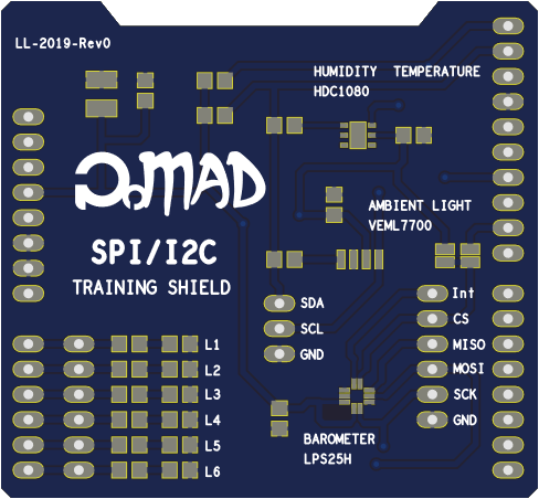
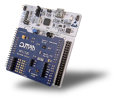
For school students, a custom shield has been developed:
 |
 |
According to the Shield Schematics, I2C and SPI line are connected to STM32 pins as follows:
| Peripheral | Line | Nucleo-64 (F072) | Nucleo-144 (F429) |
| I2C1 | SCL | PB8 (AF1) | PB8 (AF4) |
| SDA | PB9 (AF1) | PB9 (AF4) | |
| SPI1 | SCK | PB3 (AF0) | PA5 (AF5) |
| MISO | PB4 (AF0) | PA6 (AF5) | |
| MOSI | PB5 (AF0) | PA7 (AF5) | |
| GPIO | CS | PC7 | PD15 |
| INT | PB6 | PD14 |
2. I2C peripheral configuration
The code below is a basic configuration for the I2C1 peripheral. It leaves most settings to their default values. You may add this function to your bsp.c file and declare the function prototype in bsp.h.
The main concerns of the init function are:
- Configuring pins PB8 and PB9 to work as SCL and SDA in their I2C1 alternate functions (AF1)
- Make sure PB8 and PB9 output drivers are Open-Drain (important)
- Configure I2C timings. This is done by selecting the main I2C clock (from RCC), then tuning the clock prescaler, then programing the number of cycles for the clock states (high and low).
In the configuration below, we choose:
- SYSCLK = 48MHz for I2C main clock
- Prescaler = /4 to achieve a 12MHz clock
- A clock high-state delay of 60 cycles (=5µs)
- A clock low-state delay of 60 cycles (= 5µs)
The resulting clock period is 10µs, corresponding to 100kHz bus frequency. In the I2C specification, 100kHz (i.e. 100kbit/s) is referred to as the "standard mode". It is the slowest mode you'll find suitable for most available I2C devices. Yet, there is no limit in using even slower clocks. You can operate I2C at 1Hz if you like... Sometimes, it make debugging and probing easier.
/*
 * BSP_I2C1_Init()
 * Initialize I2C1 peripheral @100kHz
 */
void BSP_I2C1_Init()
{
	// Pin configuration for I2C2 pins
	// SCL -> PB8
	// SDA -> PB9

	// Enable GPIOB clock
	RCC->AHBENR |= RCC_AHBENR_GPIOBEN;

	// Configure PB8, PB9 as AF mode
	GPIOB->MODER &= ~(GPIO_MODER_MODER8 | GPIO_MODER_MODER9);
	GPIOB->MODER |= (0x02 <<16U) | (0x02 <<18U);

	// Connect to I2C1 (AF1)
	GPIOB->AFR[1] &= ~(0x000000FF);
	GPIOB->AFR[1] |=   0x00000011;

	// Setup Open-Drain
	GPIOB->OTYPER |= GPIO_OTYPER_OT_8 | GPIO_OTYPER_OT_9;

	// Select SYSCLK as I2C1 clock (48MHz)
	RCC->CFGR3 |= RCC_CFGR3_I2C1SW;

	// Enable I2C1 clock
	RCC->APB1ENR |= RCC_APB1ENR_I2C1EN;

	// Make sure I2C1 is disabled
	I2C1->CR1 &= ~I2C_CR1_PE;

	// Reset I2C1 Configuration to default values
	I2C1->CR1 	  = 0x00000000;
	I2C1->CR2 	  = 0x00000000;
	I2C1->TIMINGR = 0x00000000;

	// Configure timing for 100kHz, 50% duty cycle
	I2C1->TIMINGR |= ((4 -1) <<I2C_TIMINGR_PRESC_Pos); // Clock prescaler /4 -> 12MHz
	I2C1->TIMINGR |= (60 	 <<I2C_TIMINGR_SCLH_Pos);  // High half-period = 5µs
	I2C1->TIMINGR |= (60     <<I2C_TIMINGR_SCLL_Pos);  // Low  half-period = 5µs

	// Enable I2C1
	I2C1->CR1 |= I2C_CR1_PE;
}
3. First experiments
Let-us experiment the little code below in the main() function. As you can see, I2C is just initialized, and then we fire a START event. That's all.
int main(void)
{
	// Configure System Clock for 48MHz from 8MHz HSE
	SystemClock_Config();

	// Initialize LED and USER Button
	BSP_LED_Init();
	BSP_PB_Init();

	// Initialize Debug Console
	BSP_Console_Init();
	my_printf("\r\nConsole Ready!\r\n");
	my_printf("SYSCLK = %d Hz\r\n", SystemCoreClock);

	// Initialize I2C1 peripheral
	BSP_I2C1_Init();

	// Start I2C transaction
	I2C1->CR2 |= I2C_CR2_START;  // <-- Breakpoint here


	while(1)
	{
	}
}
In order to capture the I2C transaction, you'll need to perform the following operations very carefully:
- Save
 , build
  , and start a debug session
- Setup an oscilloscope in order to watch both SCL and SDA signals (channels 1 & 2)
- Setup the oscilloscope trigger on the falling edge of SDA
- Place a breakpoint right before the I2C transaction is fired (i.e. in front of "I2C1->CR2 |= I2C_CR2_START")
- Run the program
 up to that line, make sure that the breakpoint is reached
 - Then switch the oscilloscope into Single shot mode
- Resume program execution . This will execute I2C sequence and then get trapped in the while(1) loop
If you don't see anything on the oscilloscope, reset the program  , review your oscilloscope settings and then repeat steps 5, 6, 7. You really need to get comfortable with the above, since we're going to use it a lot in this tutorial.
If you're successful, you'll capture the beginning of the I2C transaction as shown below:
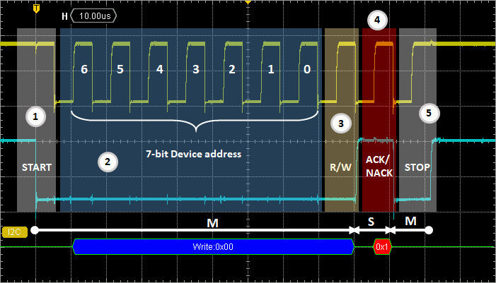
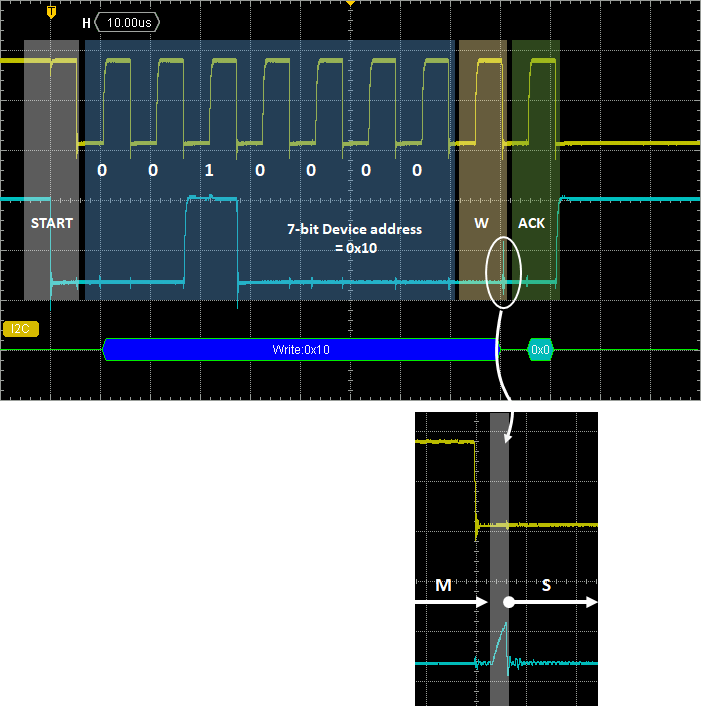
What do we have here (from left to right)?
- As specified by I2C standard, the transaction starts with a falling SDA occurring while SCL is high (START condition). Both SCL and SDA lines are controlled by the master (STM32)
- A 7-bit device address is then transmitted by the master on SDA every rising edge of SCL (0b0000000 here)
- On the 8th SCL rising edge, the master specifies if the current transaction is a READ (1) or a WRITE (0). We have a WRITE here. Write or read master modes are referred to as Master Transmitter (write) and Master Receiver (read). Practically, it just says who's taking control of SDA line after the next acknowledgement: the master (write) or the slave (read).
- On the falling edge of the 8th SCL cycle, the master turns into listening mode, reading an acknowledgement provided by the slave on the 9th SCL rising edge. Because of the pull-up resistors, a '1' here means that no device does actually acknowledge the transaction
- Since no device acknowledged, the master takes over SDA line on the falling edge of the 9th SCL cycle and stops the transaction by a rising SDA while SCL is high (STOP condition). That ends the transaction clean.
The previous transaction was not acknowledged for a simple reason: there is actually no slave device at address 0x00 on the bus. Slave address is a built-in feature for a given device model. It is provided by the manufacturer, and hence specified in the device datasheet. Assuming we want to address our light sensor, VEML7700 datasheet specifies in page 4 that I2C 7-bit address for this sensor is 0x10.
So let us try this:
int main(void)
{
	// Configure System Clock for 48MHz from 8MHz HSE
	SystemClock_Config();

	// Initialize LED and USER Button
	BSP_LED_Init();
	BSP_PB_Init();

	// Initialize Debug Console
	BSP_Console_Init();
	my_printf("\r\nConsole Ready!\r\n");
	my_printf("SYSCLK = %d Hz\r\n", SystemCoreClock);

	// Initialize I2C1 peripheral
	BSP_I2C1_Init();

	// VEML7700 slave address is 0x10
	I2C1->CR2 &= ~I2C_CR2_SADD_Msk;
	I2C1->CR2 |= ((0x10 <<1U) <<I2C_CR2_SADD_Pos);

	// Start I2C transaction
	I2C1->CR2 |= I2C_CR2_START;	  // <<-- Breakpoint here

	while(1)
	{
	}
}
Repeat above steps to capture the beginning of the I2C transaction. If you miss the capture, there is a chance you need to retry, or even unplug/replug the Nucleo® board to reset the slave I2C state machine, because the above code leaves the slave I2C decoder in an 'unfinished', waiting state, from where it may not be able to restart correctly.
This time, an existing device address is transmitted, and the expected acknowledgement bit '0' is there on the 9th SCL cycle. There is therefore no stop generated by the master and the transaction is ready for the next step in the protocol.
Getting a slave acknowledgement is very good news. It means "OK, my sensor is responding!". It is, by the way, interesting to zoom in around the falling SCL edge of the 8th cycle. This is where SDA changes from master control to slave control. The tiny spike on SDA is due to the small amount of time separating the master release from the salve takeover, pulling the '0' acknowledgment. This little spike tells you that your slave device is there, and responding! That somehow validate your hardware, your I/O settings, the communication speed, ... Very cool indeed!
OK, so far so good. What's the next step now?
An I2C or SPI slave device, whatever its purpose (a sensor, a display, a memory, a converter, an I/O extender...), is always seen from the master as a set of registers (memory locations) you can write to or read from. Each of these memory locations has an address and holds data. In the case of a sensor, you'll have to write data in some registers to configure options or turn the measure on. Then you will read results in some other registers. Pretty much like you would do with any internal peripheral indeed. This one is only external.
Most I2C/SPI devices have a register holding an identification number called 'Device ID', or 'Who Am I'. When developing communication with a new device, that's always a good start to try and read this register because you can easily check whether returned value is good or not. Unfortunately, VEML7700 has no such register. Register at address 0x00 is a configuration register that we can try and read for a start.
4. READ transaction
Page 4 of the VEML7700 datasheet specifies the 'Read' protocol. It complies with I2C standard:
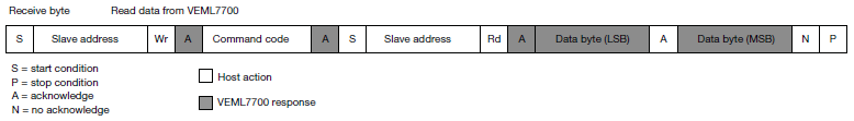
The beginning of the transaction has already been covered up to the first slave acknowledgement. The next step is to send something called the 'Command code', which basically corresponds to the register address you want to read (0x00).
Before going any further, you'll need to get familiar with the STM32 I2C peripheral, and the several status flags it features to control the transaction state machine.
Although described in the reference manual, the behavior of I2C flags is not always easy to understand. To make things more visual, we can use spare GPIOs to report 'real-time' state of some flags we want to monitor.
The first flag under interest is TXIS. Reference manual states that TXIS is set whenever I2C peripheral is waiting for a new byte to send. Remember that our next step is to send the 'Command code' 0x00. So TXIS seems to be the perfect candidate.
Let's first write a little function that waits for one or more flags to exit, while reporting the flags status on GPIO in real-time:
/*
 * Wait for & Report I2C status flags
 */

static uint8_t wait_for_flags()
{
	uint8_t	exit = 0;

	while(exit == 0)
	{
		// TXIS -> PA0
		// Exit when set
		if ((I2C1->ISR & I2C_ISR_TXIS) != 0)
		{
			GPIOA->BSRR = GPIO_BSRR_BS_0;
			exit = 1;
		}
		else GPIOA->BSRR = GPIO_BSRR_BR_0;


		// Add more flag test here
		// ...
	}

	return exit;
}
Obviously, to get this function working, you'll need to set GPIOs (PA0 for now) in Ouput Push-Pull mode. For this, I suggest adding a new BSP function called "BSP_DBG_Pins_Init()" in your bsp.c file. Remember to call this function in the init part of main().
Now edit main() to monitor TXIS flag after the transaction starts:
	// Initialize Debug pins
	BSP_DBG_Pins_Init();

	// Initialize I2C1 peripheral
	BSP_I2C1_Init();

	// VEML7700 slave address is 0x10
	I2C1->CR2 &= ~I2C_CR2_SADD_Msk;
	I2C1->CR2 |= ((0x10 <<1U) <<I2C_CR2_SADD_Pos);

	// Start I2C transaction
	I2C1->CR2 |= I2C_CR2_START;	  // <<-- Breakpoint here

	wait_for_flags();

	while(1)
	{
	}
Wire a third oscilloscope channel to PA0, then try and capture the beginning of the I2C transaction:
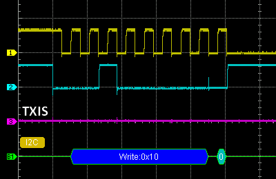
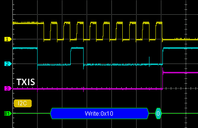
As you can see, TXIS flag is not set after the address was sent. This is because TXIS does not really tell you that you CAN send a new byte. It tells you that you MUST send a byte. How does it know that we must? We need to tell him.
This is done by filling the NBYTES field in the CR2 register. Looking back at the whole reading protocol, we can see that another START condition occurs right after the 'Command code' is sent. Therefore, the number of bytes we want to transfer for now is only one.
Try this:
	// Initialize I2C1 peripheral
	BSP_I2C1_Init();

	// VEML7700 slave address is 0x10
	I2C1->CR2 &= ~I2C_CR2_SADD_Msk;
	I2C1->CR2 |= ((0x10 <<1U) <<I2C_CR2_SADD_Pos);

	// Transfer NBYTES=1, no AUTOEND
	I2C1->CR2 &= ~I2C_CR2_NBYTES;
	I2C1->CR2 |= (1 <<16U);
	I2C1->CR2 &= ~I2C_CR2_AUTOEND;

	// Start I2C transaction
	I2C1->CR2 |= I2C_CR2_START;	  // <<-- Breakpoint here

	wait_for_flags();

	while(1)
	{
	}
Again, capture the beginning of the transaction:
This time, TXIS is set after address is sent and acknowledged. That is the event we need to proceed to the next step, sending the 'Command code' 0x00:
	// Initialize I2C1 peripheral
	BSP_I2C1_Init();

	// VEML7700 slave address is 0x10
	I2C1->CR2 &= ~I2C_CR2_SADD_Msk;
	I2C1->CR2 |= ((0x10 <<1U) <<I2C_CR2_SADD_Pos);

	// Transfer NBYTES=1, no AUTOEND
	I2C1->CR2 &= ~I2C_CR2_NBYTES;
	I2C1->CR2 |= (1 <<16U);
	I2C1->CR2 &= ~I2C_CR2_AUTOEND;

	// Start I2C transaction
	I2C1->CR2 |= I2C_CR2_START;	  // <<-- Breakpoint here

	wait_for_flags();

	// TXIS was set, proceed to sending command code
	I2C1->TXDR = 0x00;

	wait_for_flags();

	while(1)
	{
	}
Capture the transaction. You can add a test for the TC (Transfer Complete) flag in the wait_for_flag() function, with live monitoring on PA1, and an exit when set.
Then probe SCL, SDA, PA0 and PA1 with the oscilloscope. You should get this:
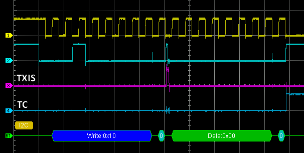
Nice!
So far, we've got 2 steps working:
- The START condition, followed by an acknowledged device address in WRITE mode.
- The rise of TXIS, indicating that a data should now be sent to the slave. Note that writing to TXDR data register automatically clears TXIS.
- After the command byte is sent, TXIS remains low (no other data to be send, because NBYTES is 1). TC rises to report that your current transfer is now complete.
Back to the 'Read' protocol, we need to re-generate a START condition, and to re-send the device address.
Because we're now entering the reading part of the transaction, let us monitor another flag: RXNE (RX Not Empty), meaning that a data has been received. Add a new test to the wait_for_flag() function with a RXNE monitor on PA1 and an exit on set. You need to keep tests on TXIS and TC for exiting, but you can remove the pin monitoring part.
		// RXNE -> PA1
		// Exit when set
		if ((I2C1->ISR & I2C_ISR_RXNE) != 0)
		{
			GPIOA->BSRR = GPIO_BSRR_BS_1;
			exit = 2;
		}
		else GPIOA->BSRR = GPIO_BSRR_BR_1;
Then edit main() in order to proceed to the I2C bus re-START in READ mode:
	// Initialize Debug pins
	BSP_DBG_Pins_Init();

	// Initialize I2C1 peripheral
	BSP_I2C1_Init();

	// VEML7700 slave address is 0x10
	I2C1->CR2 &= ~I2C_CR2_SADD_Msk;
	I2C1->CR2 |= ((0x10 <<1U) <<I2C_CR2_SADD_Pos);

	// Transfer NBYTES = 1, no AUTOEND
	I2C1->CR2 &= ~I2C_CR2_NBYTES;
	I2C1->CR2 |= (1 <<16U);
	I2C1->CR2 &= ~I2C_CR2_AUTOEND;

	// Start I2C transaction
	I2C1->CR2 |= I2C_CR2_START;	  	// <<-- Breakpoint here

	wait_for_flags();			// TXIS

	// Send command code
	I2C1->TXDR = 0x00;

	wait_for_flags();		        // TC

	// Set I2C in Read mode
	I2C1->CR2 |= I2C_CR2_RD_WRN;

	// Re-Start transaction
	I2C1->CR2 |= I2C_CR2_START;

	wait_for_flags();                       // RXNE

	// Generate STOP condition
	I2C1->CR2 |= I2C_CR2_STOP;

	while(1)
	{
	}
Generation of the STOP condition at the end is only there to close the transaction clean. Not doing so may leave the VEML7700 in an unfinished state from where you cannot easily recover.
Capture the transaction and RXNE flag on PA1. This is what you should expect:
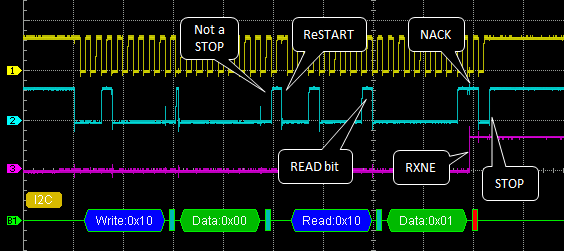
There are quite a few things to comment here:
- Remember that STOP condition is achieved by a rising SDA while SCL is high. Looking at what happens right after the second acknowledgement, you can see that SDA rises while SCL is low, therefore not creating a STOP condition before the restart (SDA falls while SCL is high). This is what we need, and the reason why we've set AUTOEND=0 before. With AUTOEND=1, a STOP would be here, breaking the whole reading process
- After the restart, the master sends the device address (0x10) again, but with the R/W bit set to 1, and the slave acknowledges. From this point, SDA is under the slave control. SCL is still driven by the master
- Because the master now plays a receiver role, it still produces SCL cycles and reads the byte from the slave (0x01 here). At the end of the 8th SCL cycle, RXNE rises, telling you that a data has been received
- On the 9th SCL cycle, the master did not acknowledge. A non-ackowledgement signal (NACK) here informs the slave that the master is done reading bytes. The slave then release SDA control back to the master
- The STOP condition is finally generated by the master
The transaction above is totally valid. The only thing is that VEML7700 has 16-bit registers, therefore a read action should be prepared to welcome 2 bytes instead of only one... That's where the NBYTES comes into the game, again.
	// Initialize Debug pins
	BSP_DBG_Pins_Init();

	// Initialize I2C1 peripheral
	BSP_I2C1_Init();

	// VEML7700 slave address is 0x10
	I2C1->CR2 &= ~I2C_CR2_SADD_Msk;
	I2C1->CR2 |= ((0x10 <<1U) <<I2C_CR2_SADD_Pos);

	// Transfer NBYTES=1, no AUTOEND
	I2C1->CR2 &= ~I2C_CR2_NBYTES;
	I2C1->CR2 |= (1 <<16U);
	I2C1->CR2 &= ~I2C_CR2_AUTOEND;

	// Start I2C transaction
	I2C1->CR2 |= I2C_CR2_START;	  	// <<-- Breakpoint here

	wait_for_flags();			// TXIS

	// Send command code
	I2C1->TXDR = 0x00;

	wait_for_flags();			// TC

	// Set I2C in Read mode
	I2C1->CR2 |= I2C_CR2_RD_WRN;

	// Transfer NBYTES=2, no AUTOEND
	I2C1->CR2 &= ~I2C_CR2_NBYTES;
	I2C1->CR2 |= (2 <<16U);
	I2C1->CR2 &= ~I2C_CR2_AUTOEND;

	// Re-Start transaction
	I2C1->CR2 |= I2C_CR2_START;

	wait_for_flags();			// RXNE

	// Read first byte (LSB)
	rx_data = I2C1->RXDR;

	wait_for_flags();			// RXNE

	// Read second byte (MSB)
	rx_data += (I2C1->RXDR <<8U);

	// Generate STOP condition
	I2C1->CR2 |= I2C_CR2_STOP;

	while(1)
	{
	}
To get the above working, you'll need to declare rx_data as a uint16_t.
And at last, we got the full reading transaction working, with the value of register at 0x00 being 0x0001:
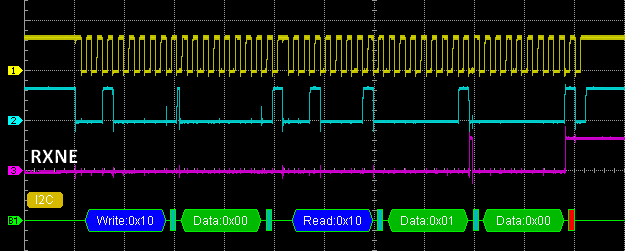
A few comments:
- Because NBYTES is now 2 during the reading phase, the first incoming byte (0x01) is now acknowledged by the master, telling the slave "keep going, I want more!".
- After the first byte is received, RXNE rises. It produces an exit from our wait_for_flags() function followed by a read of RXDR register. Reading RXDR automatically clears the RXNE flag.
- When the total number of bytes (2) have been read, the NACK is sent, and the STOP condition is generated by software.
In case you wonder, 0x0001 in VEML7700 register 0x00 just means that the sensor is actually shut down (see datasheet page 5). Clearing bit[0], in other words, writing the value 0x0000 in this register, would turn the sensor power on.
Before exploring the WRITE transaction, let us turn the READ transaction above into a more compact and generic read function. Add the following to your bsp.c/bsp.h:
uint8_t	BSP_I2C1_Read( uint8_t device_address,
                       uint8_t register_address,
                       uint8_t *buffer,
                       uint8_t nbytes )
{
	uint32_t 	timeout;	// Flag waiting timeout
	uint8_t		n;			// Loop counter

	// Set device address
	I2C1->CR2 &= ~I2C_CR2_SADD_Msk;
	I2C1->CR2 |= ((device_address <<1U) <<I2C_CR2_SADD_Pos);

        // Set I2C in Write mode
	I2C1->CR2 &= ~I2C_CR2_RD_WRN;

	// Transfer NBYTES = 1, no AUTOEND
	I2C1->CR2 &= ~I2C_CR2_NBYTES;
	I2C1->CR2 |= (1 <<16U);
	I2C1->CR2 &= ~I2C_CR2_AUTOEND;

	// Start I2C transaction
	I2C1->CR2 |= I2C_CR2_START;

	// Wait for TXIS with timeout
	timeout = 100000;
	while (((I2C1->ISR) & I2C_ISR_TXIS) != I2C_ISR_TXIS)
	{
		timeout--;
		if (timeout == 0) return 1;
	}

	// Send Register address
	I2C1->TXDR = register_address;

	// Wait for TC with timeout
	timeout = 100000;
	while (((I2C1->ISR) & I2C_ISR_TC) != I2C_ISR_TC)
	{
		timeout--;
		if (timeout == 0) return 2;
	}

	// Set I2C in Read mode
	I2C1->CR2 |= I2C_CR2_RD_WRN;

	// Transfer NBYTES, no AUTOEND
	I2C1->CR2 &= ~I2C_CR2_NBYTES;
	I2C1->CR2 |= (nbytes <<16U);
	I2C1->CR2 &= ~I2C_CR2_AUTOEND;

	// Re-Start transaction
	I2C1->CR2 |= I2C_CR2_START;

	n = nbytes;

	while (n>0)
	{
		// Wait for RXNE with timeout
		timeout = 100000;
		while (((I2C1->ISR) & I2C_ISR_RXNE) != I2C_ISR_RXNE)
		{
			timeout--;
			if (timeout == 0) return 3;
		}

		// Store data into buffer
		*buffer = I2C1->RXDR;
		buffer++;
		n--;
	}

	// Generate STOP condition
	I2C1->CR2 |= I2C_CR2_STOP;

	// Wait for STOPF with timeout
	timeout = 100000;
	while (((I2C1->ISR) & I2C_ISR_STOPF) != I2C_ISR_STOPF)
	{
		timeout--;
		if (timeout == 0) return 4;
	}

	// Return success
	return 0;
}
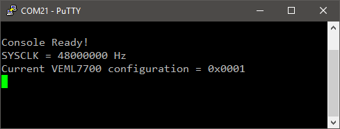
From now on, you can achieve I2C read transactions easily:
int main(void)
{
	uint8_t		rx_data[2];

	// Configure System Clock for 48MHz from 8MHz HSE
	SystemClock_Config();

	// Initialize LED and USER Button
	BSP_LED_Init();
	BSP_PB_Init();

	// Initialize Debug Console
	BSP_Console_Init();
	my_printf("\r\nConsole Ready!\r\n");
	my_printf("SYSCLK = %d Hz\r\n", SystemCoreClock);

	// Initialize I2C1 peripheral
	BSP_I2C1_Init();

	// Read 2 bytes in VEML7700 register @0x00
	BSP_I2C1_Read(0x10, 0x00, rx_data, 2);
	my_printf( "Current VEML7700 configuration = 0x%04x\r\n",
                   (uint16_t)(rx_data[1] <<8U | rx_data[0]) );

	while(1)
	{
	}
}
 |
 Commit name "I2C Read" Commit name "I2C Read" Push onto Gitlab Push onto Gitlab |
5. WRITE transaction
The WRITE transaction as provided in the VEML7700 datasheet is shown below. Again, it complies with I2C standard:

Compared to the READ sequence, writing is slightly simpler because there is no re-START involved. The master keeps controling SDA during the whole process, just listening for acknowledgements after each byte has been transferred.
You'll be interested to test and monitor some flags: TXIS, TC, and STOPF. Edit the wait_for_flags() function accordingly. Note that you must manually clear the STOPF flag before entering the test loop:
/*
 * Wait for & Report I2C status flags
 */

static uint8_t wait_for_flags()
{
	uint8_t	exit = 0;

	// Clear STOPF and NACKF flags
	I2C1->ICR |= I2C_ICR_STOPCF;
	I2C1->ICR |= I2C_ICR_NACKCF;

	while(exit == 0)
	{
		// TXIS -> PA0
		// Exit when set
		if ((I2C1->ISR & I2C_ISR_TXIS) != 0)
		{
			GPIOA->BSRR = GPIO_BSRR_BS_0;
			exit = 1;
		}
		else GPIOA->BSRR = GPIO_BSRR_BR_0;

		// TC -> PA4
		// Exit when set
		if ((I2C1->ISR & I2C_ISR_TC) != 0)
		{
			GPIOA->BSRR = GPIO_BSRR_BS_4;
			exit = 3;
		}
		else GPIOA->BSRR = GPIO_BSRR_BR_4;

		// STOPF -> PC1
		// Exit when set
		if ((I2C1->ISR & I2C_ISR_STOPF) != 0)
		{
			GPIOC->BSRR = GPIO_BSRR_BS_1;
			exit = 5;
		}
		else GPIOC->BSRR = GPIO_BSRR_BR_1;
	}

	return exit;
}
Then run the sequence below. You can put this code in main(), after the call to read function you've just made. It is an attempt to write 0x0000 in register @0x00, in order to turn the sensor power on.
	// Set device address
	I2C1->CR2 &= ~I2C_CR2_SADD_Msk;
	I2C1->CR2 |= ((0x10 <<1U) <<I2C_CR2_SADD_Pos);

	// Set I2C in Write mode
	I2C1->CR2 &= ~I2C_CR2_RD_WRN;

	// Transfer NBYTES = 3, no AUTOEND
	I2C1->CR2 &= ~I2C_CR2_NBYTES;
	I2C1->CR2 |= (3 <<16U);
	I2C1->CR2 &= ~I2C_CR2_AUTOEND;

	// Start I2C transaction
	I2C1->CR2 |= I2C_CR2_START;

	wait_for_flags();          // TXIS #1

	// Send Register address
 	I2C1->TXDR = 0x00;

	wait_for_flags();          // TXIS #2

	// Send first byte (LSB)
	I2C1->TXDR = 0x00;

	wait_for_flags();          // TXIS #3

	// Send second byte (MSB)
	I2C1->TXDR = 0x00;

	wait_for_flags();          // TC

	// Generate STOP condition
	I2C1->CR2 |= I2C_CR2_STOP;

	while(1)
	{
	}
And get the corresponding capture:
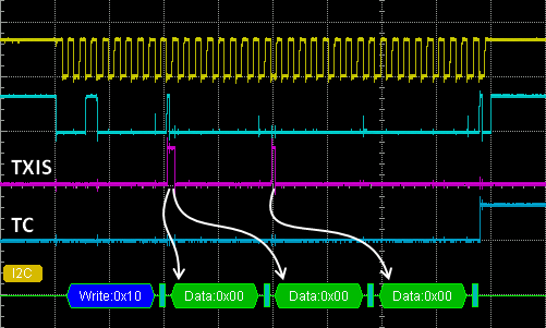
Oscilloscope shows that everything is working as expected. Yet, we can only see 2 TXIS events. There are actually 3...
First, remember that TXIS is set as soon as TXDR register is ready to accept a new byte to be transmitted.
In fact, when you load the slave register address into TXDR the first time, this data is immediately moved into the I2C peripheral internal shift register for the serial transmission over SDA to begin. That process flushes TXDR quite instantaneously, making it ready for the next load . You can therefore reload TXDR with the first data right away. But then, the shift register is busy sending the slave register address, so that TXIS is held low until the shift register is available. Once slave address has been sent over SDA, it is reloaded with the actual value of TXDR, which is the first byte of data. Doing so, the TXDR is flushed and the TXIS rises again.
Only then can you load TXDR with the second data.
Basically, you load the nth data into TXDR while the (n-1)th data is being transmitted over SDA.
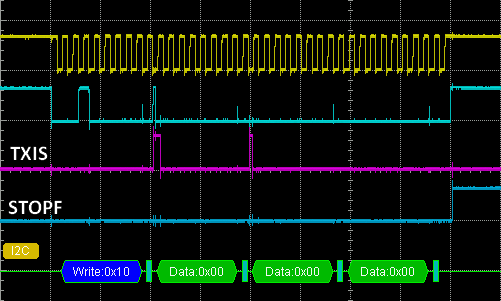
You may try something a little different, using the AUTOEND feature of the I2C peripheral:
	// Set device address
	I2C1->CR2 &= ~I2C_CR2_SADD_Msk;
	I2C1->CR2 |= ((0x10 <<1U) <<I2C_CR2_SADD_Pos);

	// Set I2C in Write mode
	I2C1->CR2 &= ~I2C_CR2_RD_WRN;

	// Transfer NBYTES = 3, with AUTOEND
	I2C1->CR2 &= ~I2C_CR2_NBYTES;
	I2C1->CR2 |= (3 <<16U);
	I2C1->CR2 |= I2C_CR2_AUTOEND;

	// Start I2C transaction
	I2C1->CR2 |= I2C_CR2_START;

	wait_for_flags();          // TXIS #1

	// Send Register address
	I2C1->TXDR = 0x00;

	wait_for_flags();          // TXIS #2

	// Send first byte (LSB)
	I2C1->TXDR = 0x00;

	wait_for_flags();          // TXIS #3

	// Send second byte (MSB)
	I2C1->TXDR = 0x00;

	wait_for_flags();          // STOPF

	while(1)
	{
	}
You pretty much obtain the same sequence as above. The only difference is that END condition is now automatically generated after 3 bytes have been transferred. If you take a look at TC flag, nothing happens after the transfer ends. In this case, the STOPF flag is set instead:
Finally, you can pack the above code into a more generic function into the bsp.c/bsp.h peripheral library:
uint8_t	BSP_I2C1_Write( uint8_t device_address,
                        uint8_t register_address,
                        uint8_t *buffer, uint8_t nbytes )
{
	uint32_t 	timeout;	// Flag waiting timeout
	uint8_t		n;		// Loop counter

	// Set device address
	I2C1->CR2 &= ~I2C_CR2_SADD_Msk;
	I2C1->CR2 |= ((device_address <<1U) <<I2C_CR2_SADD_Pos);

	// Set I2C in Write mode
	I2C1->CR2 &= ~I2C_CR2_RD_WRN;

	// Transfer NBYTES, with AUTOEND
	I2C1->CR2 &= ~I2C_CR2_NBYTES;
	I2C1->CR2 |= ((nbytes+1) <<16U);
	I2C1->CR2 |= I2C_CR2_AUTOEND;

	// Clear STOPF flag
	I2C1->ICR |= I2C_ICR_STOPCF;

	// Start I2C transaction
	I2C1->CR2 |= I2C_CR2_START;

	// Wait for TXIS with timeout
	timeout = 100000;
	while (((I2C1->ISR) & I2C_ISR_TXIS) != I2C_ISR_TXIS)
	{
		timeout--;
		if (timeout == 0) return 1;
	}

	// Send register address
	I2C1->TXDR = register_address;

	n = nbytes;

	while(n>0)
	{
		// Wait for TXIS with timeout
		timeout = 100000;
		while (((I2C1->ISR) & I2C_ISR_TXIS) != I2C_ISR_TXIS)
		{
			timeout--;
			if (timeout == 0) return 2;
		}

		// Send data
		I2C1->TXDR = *buffer;
		buffer++;
		n--;
	}

	// Wait for STOPF with timeout
	timeout = 100000;
	while (((I2C1->ISR) & I2C_ISR_STOPF) != I2C_ISR_STOPF)
	{
		timeout--;
		if (timeout == 0) return 3;
	}

	// Return success
	return 0;
}
|
Commit name "I2C Write" Push onto Gitlab |
6. Time to play!
We finally have a simple set of functions to read and write to/from I2C sensors. Your bsp.h header features:
/*
 * I2C functions
 */

void 	BSP_I2C1_Init		(void);

uint8_t	BSP_I2C1_Read		(uint8_t device_address,
                                 uint8_t register_address,
                                 uint8_t *buffer, uint8_t nbytes);

uint8_t	BSP_I2C1_Write		(uint8_t device_address,
                                 uint8_t register_address,
                                 uint8_t *buffer,
                                 uint8_t nbytes);
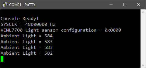
Do you see the light?
int main(void)
{
	uint8_t		rx_data[2];
	uint8_t		tx_data[0];
	uint16_t	ials;


	// Configure System Clock for 48MHz from 8MHz HSE
	SystemClock_Config();

	// Initialize LED and USER Button
	BSP_LED_Init();
	BSP_PB_Init();

	// Initialize Debug Console
	BSP_Console_Init();
	my_printf("\r\nConsole Ready!\r\n");
	my_printf("SYSCLK = %d Hz\r\n", SystemCoreClock);

	// Initialize I2C1 peripheral
	BSP_I2C1_Init();

	// VEML7700 power ON -> register @0x00
	tx_data[1] = 0x00; tx_data[0] = 0x00;
	BSP_I2C1_Write(0x10, 0x00, tx_data, 2);

	// Read VEML7700 Current configuration -> register @0x00
	BSP_I2C1_Read(0x10, 0x00, rx_data, 2);
	my_printf("VEML7700 Config = 0x%04x\r\n",(rx_data[1]<<8U | rx_data[0]));

	while(1)
	{
		// Read VEML7700 ALS (Ambient Light Sensor) -> register @0x04
		BSP_I2C1_Read(0x10, 0x04, rx_data, 2);
		ials = (rx_data[1]<<8U) | rx_data[0];
		my_printf("Ambient Light = %d\r\n", ials);

		BSP_DELAY_ms(200);
	}
}
|
Commit name "I2C Final" Push onto Gitlab |
Add new comment