
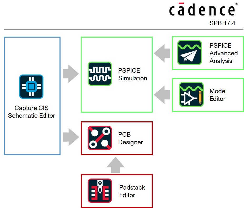
This tutorial section covers part of the Cadence® SPB design environment. SPB stands for Silicon Package Board and is the name given to a complete schematic to PCB design flow, including electrical simulation. Cadence® environment for PCB design is an assembly of software tools, each having a separate history.
For a majority of school projects, you'll need to get comfortable with only a few of these tools, namely:
- Capture CIS is used to enter/edit electrical schematics. Schematics are entry point for several subsequent tasks such as simulation or PCB design
- PSPICE AMS for analog/mixed simulation, and associated Advanced Analysis module, and the Model Editor
- PCB Designer for printed circuit board development, and associated Padstack Editor
After completing these tutorials, you should be able to:
- Edit electronic schematics
- Create libraries to manage your own parts (devices), for component that are not included in Cadence libraries
- Associate SPICE models from external sources to your own parts
- Perform standard simulations of analog circuits based on usual analysis (BIAS, DC Sweep, TRAN, AC), including parametric analysis
- Perform advanced analysis such as SENSITIVITY and MONTE-CARLO to evaluate the robustness of your schematic
- Design PCB footprints
- Design professional PCBs
- Produce fabrication files for PCBs (GERBERS, DRILL)
- Create 3D models of assembled boards for further mechanical integration
In short, a few things an electrical engineer is supposed to master when it comes to hardware design.
Tutorials have been updated and tested with the SPB 17.4 release (2021)