
Integrated Circuit with bottom pads
More difficult now ! This tutorial addresses the soldering of a Quad Flat No-lead package (QFN). As the name tells us, there is no lead pins. Connections are made by pads located on the bottom surface of the package.
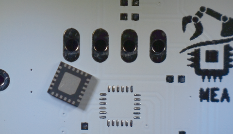
The picture below shows a 3x3mm QFN package and the targeted footprint. Note that the footprint misses the central pad. Soldering of the central pad is not always "electrically mandatory". In some cases, QFN central pad is there for thermal and mechanical concerns only. It's clearly not recommended to leave this pad without soldering, although this makes the DIY process a little bit easier.
The secret for soldering success lies in the preparation of both the footprint and the device. Be patient, use flux, bring tin, clean with alcohol, and repeat until both footprint and device are ready for final reflow.
Step 1: Prepare the PCB footprint. That part is pretty easy using flux.
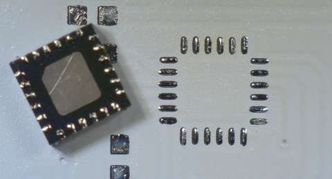
Step 2: Prepare the device. Basically it is the same process as above. You need some kind of setup to hold the device during operation. Here, I'm using inverted tweezers and third hand tool to keep the device (barely) steady. You can change device orientation in the tweezers to get easy access of all edges. The most difficult thing, in the demo below, is to avoid wetting the central pad. In most cases, you'll want to wet the central pad altogether with the ring pads. If so, carefully keep the amount of tin on the central pad very low. Basically you want the same tin thickness everywhere. A higher bump on the central pad prevents good soldering of the ring pads because the device will be center-lifted. If there's too much tin somewhere, use desoldering braid. Again, be patient.
Use alcohol to clean up the device when you're done.
At this step, you have a clean prepared footprint, and a clean prepared device. All is well, you've done the most difficult part.
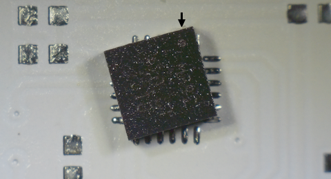
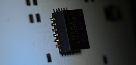
Locate the device pin #1 and prepare correct device orientation:
Step 3: Let the magic operate! Try to keep the device centered on the footprint with very light tweezers action and apply a very gentle, hot air flow. It takes some time to get all the pins reflow but if you pay attention, you can see the very moment the device goes self-centered by melted tin surface tension. You need to relax pressure on the tweezers as reflow goes on. That's the trickiest part...
Wait some seconds for cooling down and make sure that the device is perfectly laid down flat on the PCB:
You may want to rework/reflow pads you feel missing some tin:
Beautiful:
Add new comment